Silicon carbide planar MOSFET device and preparation method thereof
A silicon carbide and device technology, applied in semiconductor/solid-state device manufacturing, semiconductor devices, electrical components, etc., to achieve the effects of reducing leakage current, large forward and reverse symmetrical withstand voltage, and large reverse withstand voltage
- Summary
- Abstract
- Description
- Claims
- Application Information
AI Technical Summary
Problems solved by technology
Method used
Image

Examples
Embodiment 1
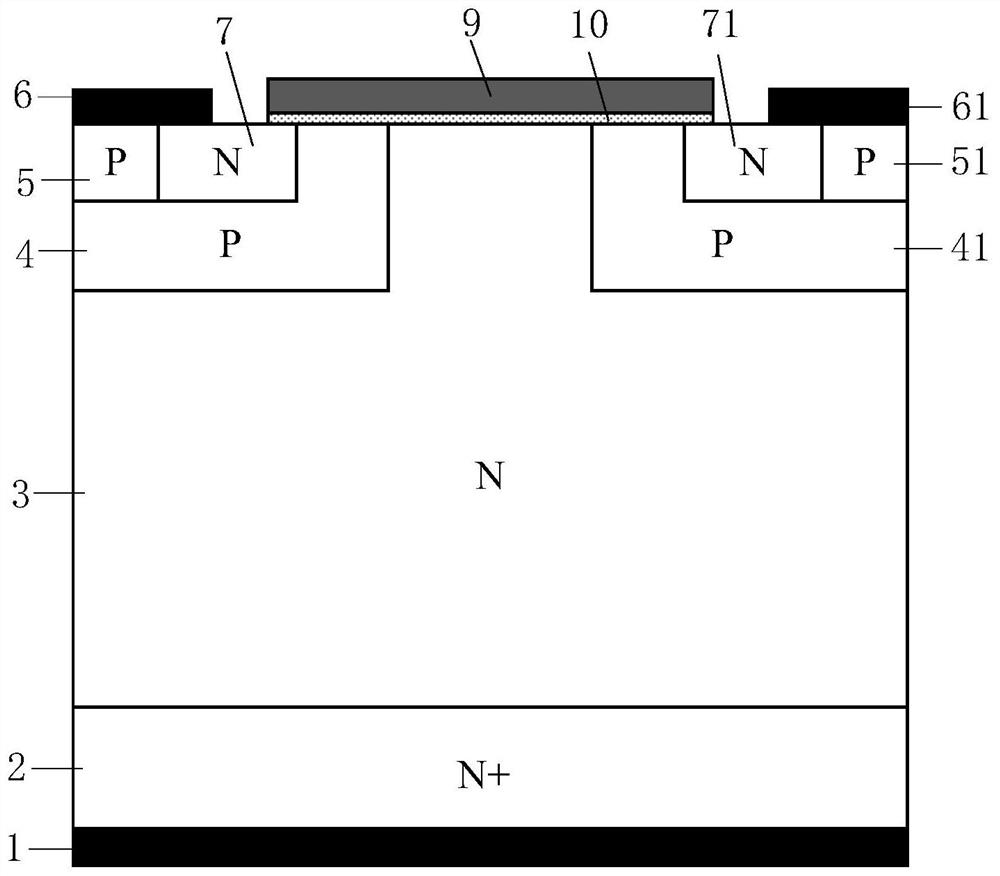
[0106] A silicon carbide planar MOSFET device, its cell structure is as follows figure 2 As shown, its half-cell structure includes a back drain metal 1, a second N-type silicon carbide buffer layer 21, and an N-type silicon carbide epitaxial layer 3, which are sequentially stacked from bottom to top.
[0107] Above the N-type silicon carbide epitaxial layer 3 is the first N-type silicon carbide buffer layer 11, the first N-type silicon carbide buffer layer 11 includes a vertical section in the middle and horizontal sections on both sides, the first N-type silicon carbide buffer layer 11 The upper left is the first P-type base region 4, inside the first P-type base region 4 is the first P-type source region 5 and the first N-type source region 7, the first P-type source region 5 and the first N-type source region The region 7 is connected left and right, and the first source metal 6 is respectively connected to the first P-type source region 5 and part of the first N-type sou...
Embodiment 2
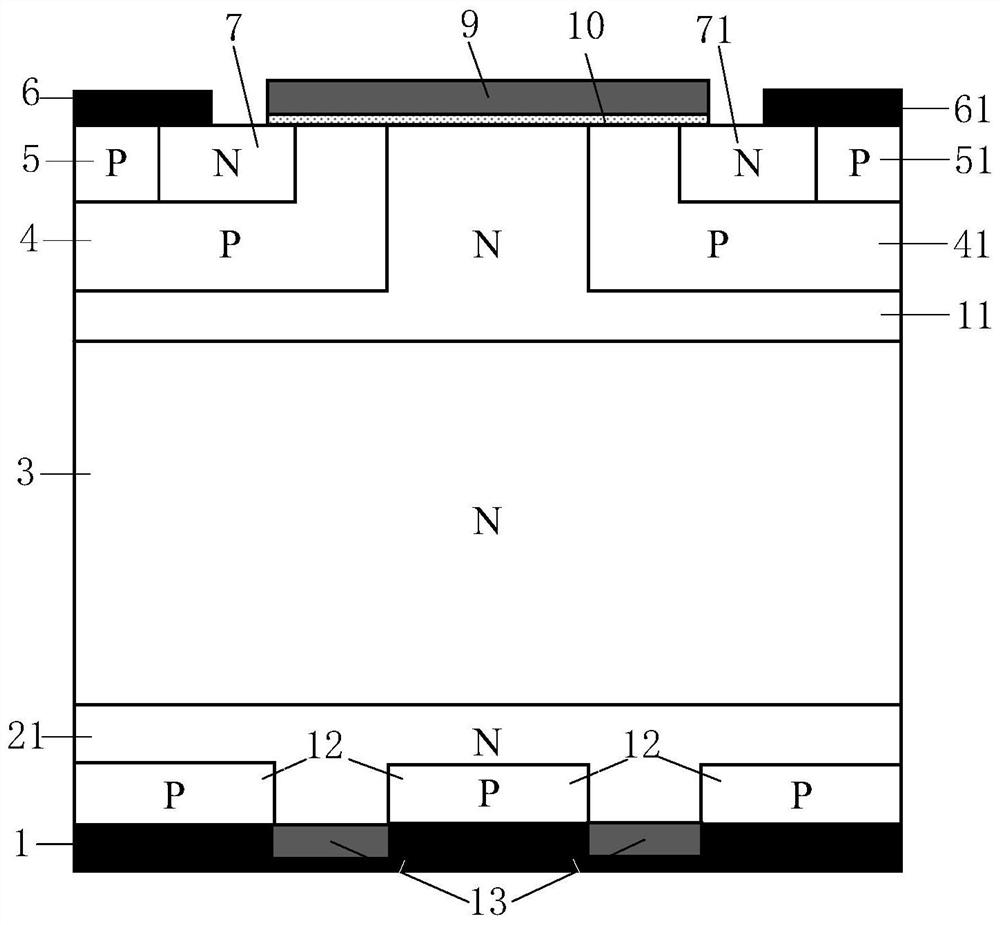
[0125] A silicon carbide planar MOSFET device, its cell structure is as follows image 3 shown, including:
[0126] Its half-cell structure includes a back drain metal 1, a second N-type silicon carbide buffer layer 21, and an N-type silicon carbide epitaxial layer 3 stacked sequentially from bottom to top.
[0127]Above the N-type silicon carbide epitaxial layer 3 is the first N-type silicon carbide buffer layer 11, the first N-type silicon carbide buffer layer 11 includes a vertical section in the middle and horizontal sections on both sides, the first N-type silicon carbide buffer layer 11 The upper left is the first P-type base region 4, inside the first P-type base region 4 is the first P-type source region 5 and the first N-type source region 7, the first P-type source region 5 and the first N-type source region The region 7 is connected left and right, and the first source metal 6 is respectively connected to the first P-type source region 5 and part of the first N-typ...
Embodiment 3
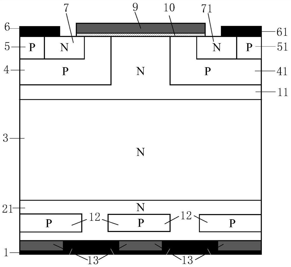
[0146] A silicon carbide planar MOSFET device such as Figure 4 As shown, its cellular structure includes:
[0147] Its half-cell structure includes a back drain metal 1, a second N-type silicon carbide buffer layer 21, and an N-type silicon carbide epitaxial layer 3 stacked sequentially from bottom to top.
[0148] Above the N-type silicon carbide epitaxial layer 3 is the first N-type silicon carbide buffer layer 11, the first N-type silicon carbide buffer layer 11 includes a vertical section in the middle and horizontal sections on both sides, the first N-type silicon carbide buffer layer 11 The upper left is the first P-type base region 4, inside the first P-type base region 4 is the first P-type source region 5 and the first N-type source region 7, the first P-type source region 5 and the first N-type source region The region 7 is connected left and right, and the first source metal 6 is respectively connected to the first P-type source region 5 and part of the first N-ty...
PUM
 Abstract
Description
Claims
Application Information
 - R&D Engineer
- R&D Manager
- IP Professional
- Industry Leading Data Capabilities
- Powerful AI technology
- Patent DNA Extraction
Browse by: Latest US Patents, China's latest patents, Technical Efficacy Thesaurus, Application Domain, Technology Topic.
© 2024 PatSnap. All rights reserved.Legal|Privacy policy|Modern Slavery Act Transparency Statement|Sitemap