Multi-bare-chip package structure, chip and method

A packaging structure and multi-die technology, which is applied in semiconductor/solid-state device parts, semiconductor devices, electrical components, etc., can solve the problems of high production cost, achieve the effect of reducing parasitic impedance and cost

Pending Publication Date: 2021-04-27
CHENGDU MONOLITHIC POWER SYST
View PDF4 Cites 0 Cited by
  • Summary
  • Abstract
  • Description
  • Claims
  • Application Information

AI Technical Summary

Problems solved by technology

Therefore, this single die is expensive to manufacture due to the fact that the switching device and the controller are manufactured together.

Method used


Image

  • Multi-bare-chip package structure, chip and method
  • Multi-bare-chip package structure, chip and method
  • Multi-bare-chip package structure, chip and method

Examples


Embodiment Construction

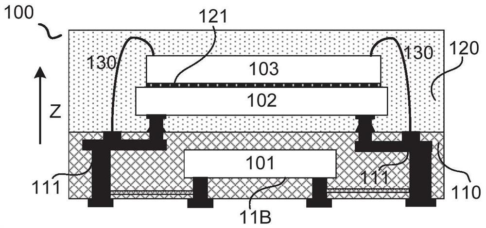
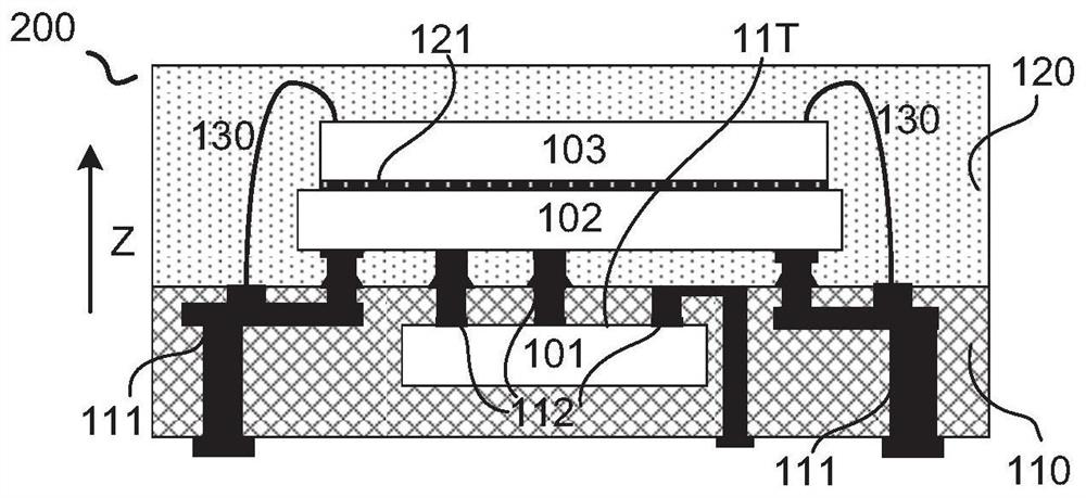
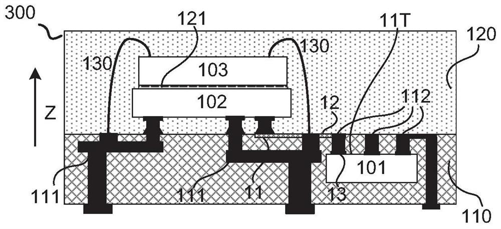
[0017] Specific embodiments of the present invention will be described in detail below, and it should be noted that the embodiments described here are only for illustration, not for limiting the present invention. In the following description, numerous specific details are set forth in order to provide a thorough understanding of the present invention. It will be apparent, however, to one of ordinary skill in the art that these specific details need not be employed to practice the present invention. In other instances, well-known circuits, materials or methods have not been described in detail in order to avoid obscuring the present invention.

[0018] Throughout this specification, reference to "one embodiment," "an embodiment," "an example," or "example" means that a particular feature, structure, or characteristic described in connection with the embodiment or example is included in the present invention. In at least one embodiment. Thus, appearances of the phrases "in on...


PUM


Abstract

The invention discloses a multi-bare-chip packaging structure, a chip and a method. The multi-bare-chip packaging structure comprises: an embedded bare chip which is buried in a substrate; a flip bare chip which is placed above the substrate and is electrically connected with the substrate through a conductor; and a bonding bare chip which is bonded above the flip bare chip and is electrically connected with the substrate through a bonding wire. According to the multi-bare-chip packaging structure, the cost is reduced, and the performance is improved.

Description

technical field [0001] The present invention relates to a semiconductor package, and more specifically, the present invention relates to a multi-die package structure, chip and method. Background technique [0002] The requirements of client electronics have increased significantly in recent years. Miniaturization and portability are unstoppable trends, driving more compact chip packages. Correspondingly, while portable electronic devices have more functions and better performance, their volumes are becoming smaller and smaller. Therefore, today's power supply systems are required to have smaller size, higher power output, more functions and higher efficiency. Under these requirements, some technologies integrate switching devices such as field effect transistors and controllers into a single die. However, generally speaking, the controller uses a complementary metal-oxide-semiconductor process (CMOS process), which requires 18 to 20 mask manufacturing processes; while th...

Claims


Application Information

Patent Timeline
Patent Type & Authority Applications(China)
IPC IPC(8): H01L23/31H01L25/065H01L21/56
CPCH01L23/3121H01L25/0657H01L21/563H01L2225/0651H01L23/3128H01L24/49H01L2224/16225H01L2224/73265H01L2224/32145H01L2224/48227H01L2924/00014H01L2924/181H01L2924/15192H01L2224/73253H01L24/19H01L24/20H01L2224/16235H01L2224/48235H01L24/48H01L24/16H01L24/32H01L24/73H01L2224/13101H01L2224/13082H01L2224/83191H01L24/83H01L2224/48091H01L23/5389H01L2224/04105H01L2224/12105H01L2224/16145H01L2224/16227H01L2225/06517H01L2225/06513H01L25/0652H01L2924/00012H01L2224/45099H01L2924/014H01L21/56H01L23/5383H01L25/50
Inventor 蒲应江蒋航
Owner CHENGDU MONOLITHIC POWER SYST
Why Eureka
Try Eureka