Supercharge Your Innovation With Domain-Expert AI Agents!

Dual-depth via device and process for large back contact solar cells

A technology of depth and contact, applied in electrical components, semiconductor devices, circuits, etc., can solve problems such as unavailability and high price

Pending Publication Date: 2021-04-30
阵列光子学公司
View PDF12 Cites 2 Cited by
  • Summary
  • Abstract
  • Description
  • Claims
  • Application Information

AI Technical Summary

Problems solved by technology

Large area PCBs with sufficiently low CTE are either not available or expensive

Method used


Image

  • Dual-depth via device and process for large back contact solar cells
  • Dual-depth via device and process for large back contact solar cells
  • Dual-depth via device and process for large back contact solar cells

Examples


Embodiment Construction

[0034] The following detailed description refers to the accompanying drawings that show, by way of illustration, specific details and embodiments in which the invention may be practiced. These embodiments are described in sufficient detail to enable those skilled in the art to practice the invention. Other embodiments may be utilized and structural, logical, and electrical changes may be made without departing from the scope of the present invention. The various embodiments disclosed herein are not necessarily mutually exclusive, as some disclosed embodiments can be combined with one or more other disclosed embodiments to form new embodiments. Accordingly, the following detailed description should not be taken in a limiting sense, and the scope of embodiments of the present invention is defined only by the appended claims along with the full scope of equivalents to which such claims are entitled.

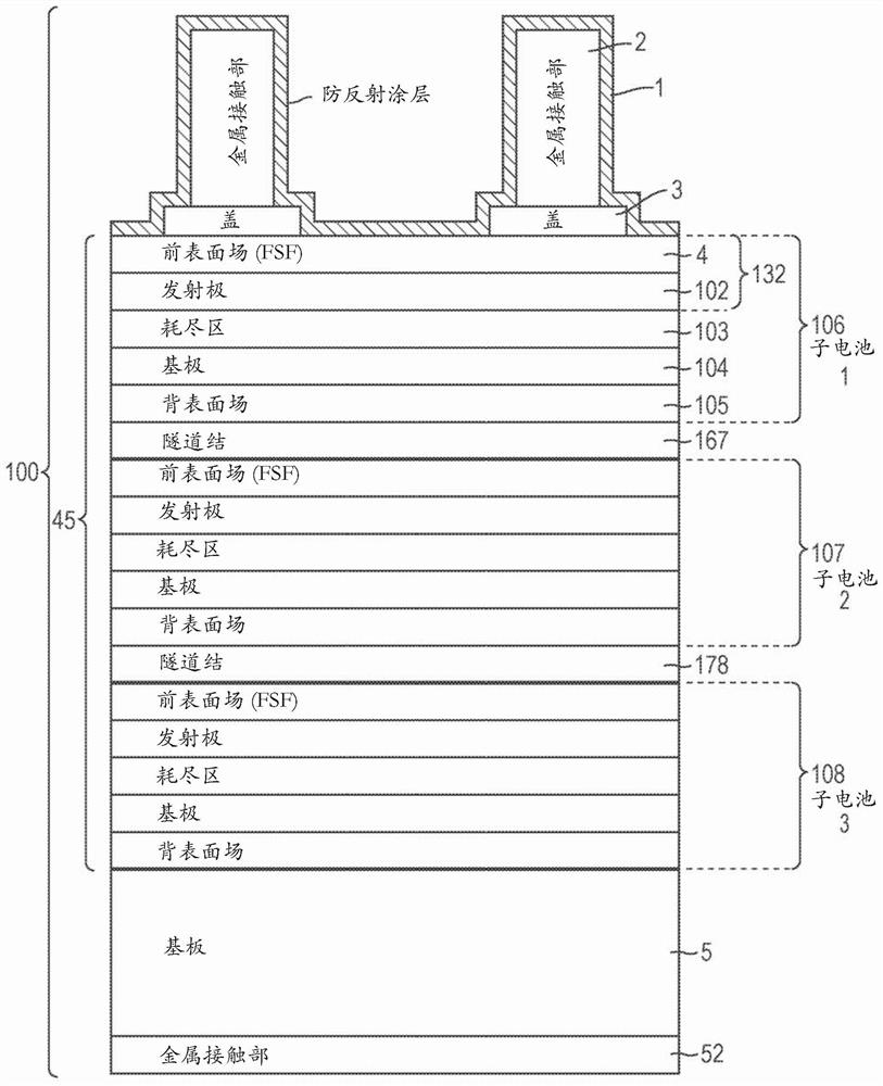
[0035] Conventional multijunction solar cells have been widely used in terrest...


PUM

PropertyMeasurementUnit
thicknessaaaaaaaaaa
thicknessaaaaaaaaaa
tensile strengthaaaaaaaaaa

Abstract

Dual-depth through-wafer-via semiconductor devices and methods for fabricating dual-depth through-wafer-via semiconductor devices are disclosed. In particular, back- contact-only multijunction photovoltaic cells and the process flows for making such cells are disclosed. The dual-depth through-wafer-via multijunction photovoltaic cells include through-wafer-vias for interconnecting the front surface epitaxial layer to a contact pad on the back surface. Before etching the through-wafer-vias the substrate is thinned to less than 150 pm. The dual-depth through-wafer-vias are formed using a two-step wet etch process that removes semiconductor materials non-selectively without major differences in etch rates between heteroepitaxial III-V semiconductor layers. Low-stress passivation layers are used to reduce the thermo-mechanical stress of the semiconductor devices. A bypass diode is integrated in the recess on the backside formed by the dual-depth through-wafer structure.

Description

technical field [0001] The present disclosure relates to photovoltaic cells, methods for manufacturing photovoltaic cells, methods for assembling solar panels, and solar panels including photovoltaic cells. In particular, the present disclosure relates to multi-junction photovoltaic cells with through-wafer vias and discrete bypass diodes integrated onto the backside. The multi-junction photovoltaic cell includes dual-depth through-wafer vias for interconnecting the front surface epitaxial layers to contact pads on the back surface and for providing recesses on the backside to allow mounting of bypass diodes. The dual-depth through-wafer vias are formed using a two-step wet etch process that removes portions of the substrate and then non-selectively removes the semiconductor without significant differences in etch rates between heteroepitaxial III-V semiconductor layers Material. A low stress passivation layer is used to improve device reliability over a wide temperature ran...

Claims


Application Information

Patent Timeline
Patent Type & Authority Applications(China)
IPC IPC(8): H01L31/18H01L31/08
CPCH01L31/0443H01L31/0725H01L31/02245H01L31/0516Y02E10/50H01L31/02008H01L31/048
Inventor L·张
Owner 阵列光子学公司
Features
  • R&D
  • Intellectual Property
  • Life Sciences
  • Materials
  • Tech Scout
  • Unparalleled Data Quality
  • Higher Quality Content
  • 60% Fewer Hallucinations
Learn More