BGA packaging solder ball detection system and method

A detection system and detection method technology, applied in measurement devices, optical devices, optical testing flaws/defects, etc., can solve problems such as constraints and lack of height information, and achieve efficient access integration, accurate and efficient acquisition, accuracy and stability The effect of detection ability

Inactive Publication Date: 2021-05-04
VOMMA (SHANGHAI) TECH CO LTD
View PDF11 Cites 4 Cited by
  • Summary
  • Abstract
  • Description
  • Claims
  • Application Information

AI Technical Summary

Problems solved by technology

At present, the three-dimensional size measurement and defect detection of BGA solder balls in the industry are mostly carried out by manual re-judgment after two-dimensional camera detection. Although it has advantages in solder ball positioning, due to the lack of height information, it can only judge the solder at the corresponding position from a certain angle. The detection of solder volume, surface roundness, foreign matter and other adverse phenomena in various complex situations still relies on manual re-judgment and random inspection, which has caused serious restrictions on the automatic networking in electronic production

Method used


Image

  • BGA packaging solder ball detection system and method
  • BGA packaging solder ball detection system and method
  • BGA packaging solder ball detection system and method

Examples


Embodiment Construction

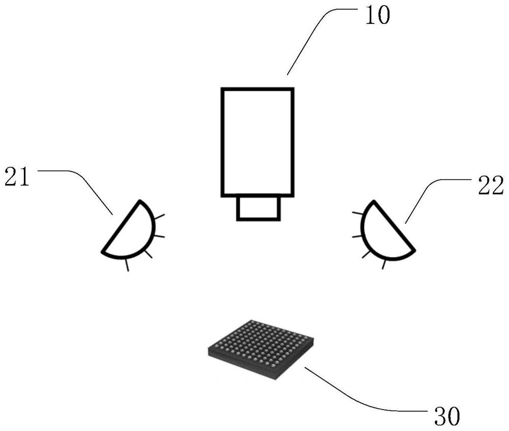
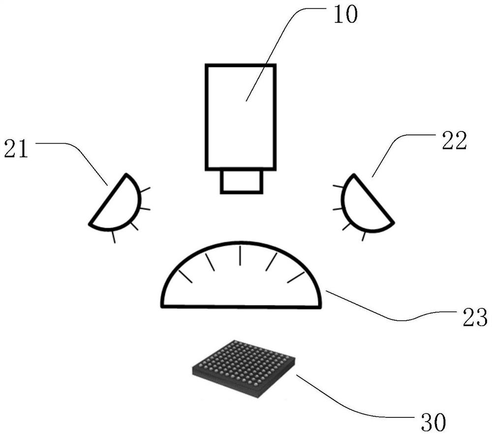
[0025] According to one or more embodiments, such as image 3 As shown, a BGA packaging solder ball detection system, the detection system includes a light field camera, the lens of the light field camera is the BGA package solder ball to be detected, for obtaining the image of the solder ball; two light sources, The light from the two light sources is directed to the BGA package solder balls, and is used to help the light field camera to obtain an image of the solder balls.

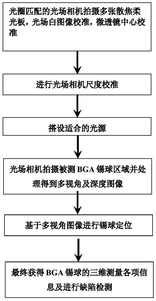
[0026] According to one or more embodiments, such as figure 1 As shown, a BGA packaging solder ball detection system, the detection system for the detection process of the solder ball includes,

[0027] Adjusting the focal length and / or aperture of the light field camera to obtain a plurality of defocused soft light pure color calibration plates of the BGA package solder balls to obtain a light field white image of the solder balls;

[0028] Calibrate the white image of the light field, and calibrate t...


PUM


Abstract

A BGA packaging solder ball detection system comprises a light field camera and a light source, wherein a lens faces a to-be-detected BGA packaging solder ball, and the light field camera is used for acquiring an image of the solder ball; and the light source emits light to the BGA packaging solder ball and is used for helping the light field camera to obtain an image of the solder ball. The detection process of the solder ball comprises the following steps of: adjusting the focal length and / or aperture of the light field camera, acquiring a plurality of defocused soft light pure color calibration plates of the BGA packaging solder ball, and acquiring a light field white image of the solder ball; calibrating the light field white image, and calibrating the center of a micro lens of the light field camera; performing scale calibration on the light field camera; erecting and adjusting the light source; shooting a to-be-detected BGA solder ball region array through using the light field camera to obtain a multi-view image and a depth image; according to the light field multi-view image and the depth image, carrying out position identification and positioning of the solder ball; and finally, acquiring three-dimensional size measurement information and defect detection information of the detected solder ball.

Description

technical field [0001] The invention belongs to the technical field of integrated circuit package measurement, in particular to a BGA package solder ball detection system and method. Background technique [0002] In recent years, with the rapid growth of science and technology and industrial level, the requirements for electronic products in daily life are getting higher and higher, and the demand is also increasing. The ball grid array packaging solder ball BGA technology of integrated circuit chips has improved the production speed of circuit boards to a certain extent. However, with the development of precision packaging, the requirements for solder balls are relatively strict, so the detection speed of solder balls has become a key factor restricting this technology. Photoelectric detection technology can be used for three-dimensional dimension measurement and defect detection of ball grid array packaging solder balls (English: BGA, Ball Grid Array, hereinafter referred...

Claims


Application Information

Patent Timeline
Patent Type & Authority Applications(China)
IPC IPC(8): G01B11/00G01N21/01G01N21/88
CPCG01B11/00G01N21/01G01N21/8851G01N2021/0112G01N2021/8887
Inventor 丁俊飞李浩天
Owner VOMMA (SHANGHAI) TECH CO LTD
Why Eureka
Try Eureka