Clamping device for circuit board machining

A clamping device and circuit board technology, which is applied in the directions of printed circuits, printed circuit manufacturing, and assembling printed circuits with electrical components, can solve the problems of troublesome operation, insufficient friction, affecting the installation of electronic components, etc., and achieves convenient solder processing, Avoid troublesome operation and ensure the effect of stability

Inactive Publication Date: 2021-05-04
吴日香
View PDF0 Cites 5 Cited by
  • Summary
  • Abstract
  • Description
  • Claims
  • Application Information

AI Technical Summary

Problems solved by technology

[0003] However, when the substrate is clamped and fixed, it is usually clamped by sliding the clamps on both sides to the side close to each other. In the case that the other two sides of the substrate are not limited and clamped, it is often caused by the clamps and the side of the substrate. The lack of friction between the walls causes the substrate to slide on a horizontal plane, which affects the installation of electronic components on the substrate, and after inserting the pins of the electronic components through the specified position of the substrate, in order to solder the back of the substrate, it is necessary to The substrate is disassembled, and the substrate is manually turned over and then re-fixed. The operation is cumbersome and reduces the processing efficiency of the circuit board. Electronic components are squeezed and fixed, and soldering can only be performed with one hand, which is not only inconvenient to operate, but also affects the accuracy of soldering

Method used


Image

  • Clamping device for circuit board machining
  • Clamping device for circuit board machining
  • Clamping device for circuit board machining

Examples


Embodiment Construction

[0028] In order to make the technical means, creative features, goals and effects achieved by the present invention easy to understand, the present invention will be further described below in conjunction with specific embodiments.

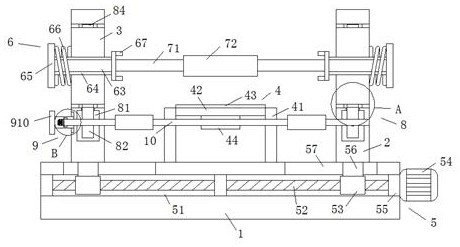
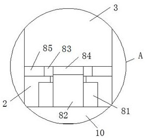
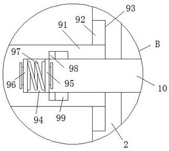
[0029] Such as Figure 1-Figure 9 As shown, a clamping device for circuit board processing according to the present invention includes a processing table 1, a sliding splint 2, a fixed turntable 3, an extrusion mechanism 4, a driving mechanism 5, a first clamping mechanism 6, and a second clamping mechanism. A holding mechanism 7, a rotating mechanism 8, a fixing mechanism 9 and an electronic telescopic rod 10, a sliding splint 2 is slidably connected to both sides of the upper end of the processing table 1, and a sliding splint 2 is rotatably connected to the sliding splint 2 and above the sliding splint 2. A fixed turntable 3, the electronic telescopic rod 10 is rotatably connected between the two sliding splints 2 and located below the fixed tu...


PUM


Abstract

The invention relates to the field of circuit board machining, in particular to a clamping device for circuit board machining, which comprises a machining table, sliding clamping plates, a fixed turntable, an extrusion mechanism, a driving mechanism, a first clamping mechanism, a second clamping mechanism, a rotating mechanism, a fixing mechanism and an electronic telescopic rod, wherein the two sides of the upper end of the machining table are each slidably connected with one sliding clamping plate, and a fixed rotating disc is rotationally connected to the sliding clamping plates and located above the sliding clamping plates. Through rotation of a threaded rod of the driving mechanism, the two sliding clamping plates and the fixed rotating disc can be driven to slide towards the sides close to each other, so that two fixed clamps of the first clamping mechanism can be driven to slide towards the sides close to each other, a connecting rotating rod of the second clamping mechanism can be pushed to rotate, the two fixing clamps and two limiting clamping frames are used for fixing and clamping the four edges of a circuit board, so that the stability of the circuit board in the machining process can be guaranteed, and the circuit board is prevented from sliding on a plane.

Description

technical field [0001] The invention relates to the field of circuit board processing, in particular to a clamping device for circuit board processing. Background technique [0002] The circuit board is a circuit board with FPC characteristics and PCB characteristics formed by combining a flexible circuit board and a rigid circuit board through lamination and other processes according to relevant process requirements. It is usually composed of a substrate and various electronic components fixed on the substrate. Component composition. During the production process, the metal pins of the electronic components are usually inserted into the designated positions on the front of the substrate, and then the substrate is turned over, and the metal pins of the electronic components passing through the substrate are soldered and fixed on the rear side of the substrate. [0003] However, when the substrate is clamped and fixed, it is usually clamped by sliding the clamps on both sides...

Claims


Application Information

Patent Timeline
Patent Type & Authority Applications(China)
IPC IPC(8): H05K3/34
CPCH05K3/3447H05K2203/0165H05K2203/1563
Inventor 吴日香
Owner 吴日香
Why Eureka
Try Eureka