Unlock instant, AI-driven research and patent intelligence for your innovation.

Implementation method for high-speed programming of embedded flash memory and programming system of embedded flash memory

An implementation method and programming system technology, applied in the field of embedded flash memory programming, can solve the problems of time overhead, low efficiency, time-consuming, etc., and achieve the effect of avoiding time overhead and improving programming efficiency

Active Publication Date: 2021-05-14
上海灵动微电子股份有限公司
View PDF12 Cites 0 Cited by
  • Summary
  • Abstract
  • Description
  • Claims
  • Application Information

AI Technical Summary

Problems solved by technology

The access speed of the core registers is very slow, and at the same time, it takes time for the MCU to go from the stop state to the running state. After multiple rounds of programming operations, it causes a problem of time-consuming and low efficiency, and cannot cope with complex programming situations well.
[0004] Thereby, existing FLASH programming implementation method still needs to be improved and increase

Method used


Image

  • Implementation method for high-speed programming of embedded flash memory and programming system of embedded flash memory
  • Implementation method for high-speed programming of embedded flash memory and programming system of embedded flash memory
  • Implementation method for high-speed programming of embedded flash memory and programming system of embedded flash memory

Examples


Embodiment Construction

[0034] In the following description, many technical details are proposed in order to enable readers to better understand the application. However, those skilled in the art can understand that the technical solutions claimed in this application can be realized even without these technical details and various changes and modifications based on the following implementation modes.

[0035] In order to make the purpose, technical solution and advantages of the present application clearer, the implementation manner of the present application will be further described in detail below in conjunction with the accompanying drawings.

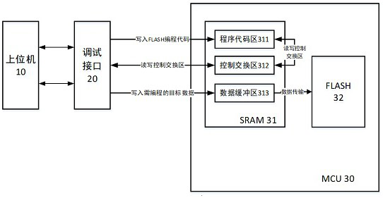
[0036] The first embodiment of the present application discloses a method for implementing high-speed programming of embedded flash memory, which is used to implement programming of flash memory in a programming system. figure 1 A schematic structural diagram of a programming system is shown, and the programming system includes a host computer 10 , a debug...


PUM


Abstract

The invention relates to an implementation method for high-speed programming of an embedded flash memory and a programming system, the system comprises an upper computer, a debugging interface and a microcontroller, the microcontroller comprises a static memory and a flash memory, and the static memory comprises a program code area, a control exchange area and a data buffer area. The upper computer obtains parameters of the static memory and the flash memory and writes flash memory programming codes into a program code area; the microcontroller operates flash memory programming codes in the program code area and writes a normal operation mark into the control exchange area; the upper computer reads the normal operation mark, configures a write-in address of the data in the flash memory, transmits the to-be-written data to a data buffer area, and writes an operation command into a control exchange area; the microcontroller reads an operation command and a write-in address, writes the data to be written in the data buffer area into the flash memory, and then writes an operation result and a programming result response in the control exchange area; the upper computer obtains a programming result response, and modifies the write-in address according to the size of the data written into the flash memory; and the microcontroller is not interrupted in the operation process of the programming system.

Description

technical field [0001] The present application relates to the field of embedded flash memory programming, and further relates to a method for implementing high-speed programming of embedded flash memory and a programming system for embedded flash memory. Background technique [0002] FLASH programming is an important part of MCU debugging. After the program image is created, the program needs to be downloaded to the FLASH memory of the MCU. The debug adapter is connected to the PC through USB / Ethernet, complies with the debug protocol JTAG / serial wire debug protocol, and passes the commands sent by the debug adapter through the debug access port (DAP) of the MCU and the memory access port module (AHB-AP) Finally converted to a protocol based on the Advanced High Performance Bus (AHB), the AHB-AP module is connected to the MCU internal bus system, so that the debug adapter can access all memory, peripherals, debug components and debug registers in the processor, thus complet...

Claims


Application Information

Patent Timeline
Patent Type & Authority Applications(China)
IPC IPC(8): G11C16/10G11C16/20
CPCG11C16/20G11C16/10
Inventor 汤臻章锡翔刘强吴忠洁
Owner 上海灵动微电子股份有限公司
Features
  • R&D
  • Intellectual Property
  • Life Sciences
  • Materials
  • Tech Scout
  • Unparalleled Data Quality
  • Higher Quality Content
  • 60% Fewer Hallucinations
Learn More