Supercharge Your Innovation With Domain-Expert AI Agents!

A high-precision jig and working method for tooling to position printed circuit boards

A technology of printed circuit boards and working methods, which is applied in the direction of assembling printed circuits with electrical components, printed circuits, and printed circuit manufacturing, and can solve problems such as troublesome fixture operation, low efficiency of tooling positioning, and reduced welding accuracy of electronic components. Achieve the effects of reducing work intensity, improving welding accuracy, and improving the efficiency of positioning tooling

Active Publication Date: 2021-06-25
四川英创力电子科技股份有限公司
View PDF0 Cites 0 Cited by
  • Summary
  • Abstract
  • Description
  • Claims
  • Application Information

AI Technical Summary

Problems solved by technology

There is no structure for fixing the circuit board on the traditional jig, only a groove for the circuit board to be placed. After the printed circuit board is placed in the groove, it is necessary to stick tape around the circuit board to fix the printed circuit board , this kind of jig is cumbersome to operate, and the efficiency of tooling positioning is low
At present, a plurality of pressing plate mechanisms are installed around the jig, and the pressing plate is pressed on the top surface of the printed circuit board by rotating the pressing plate. Although this pressing plate mechanism can improve the tooling positioning efficiency of the printed circuit board, it needs to be rotated. Multiple pressure plates undoubtedly increase the labor intensity of workers and reduce the efficiency of tooling positioning of printed circuit boards
In addition, in the process of soldering electronic components, a large amount of heat is generated on the printed circuit board, and the printed circuit board is in a fixed state, which causes the printed circuit board to arch upwards, thereby reducing the welding accuracy of electronic components

Method used


Image

  • A high-precision jig and working method for tooling to position printed circuit boards
  • A high-precision jig and working method for tooling to position printed circuit boards
  • A high-precision jig and working method for tooling to position printed circuit boards

Examples


Embodiment Construction

[0024] The present invention will be further described below in conjunction with accompanying drawing, protection scope of the present invention is not limited to the following:

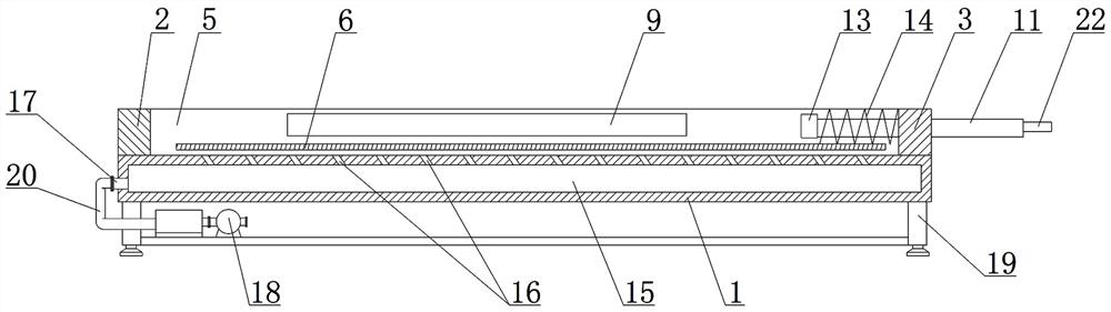
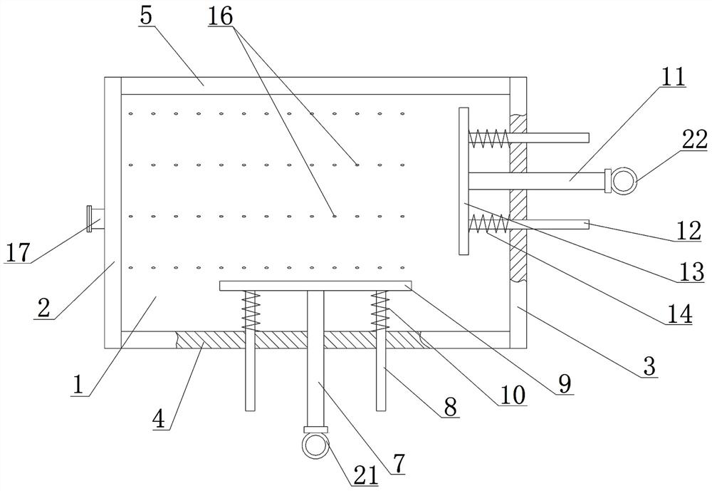
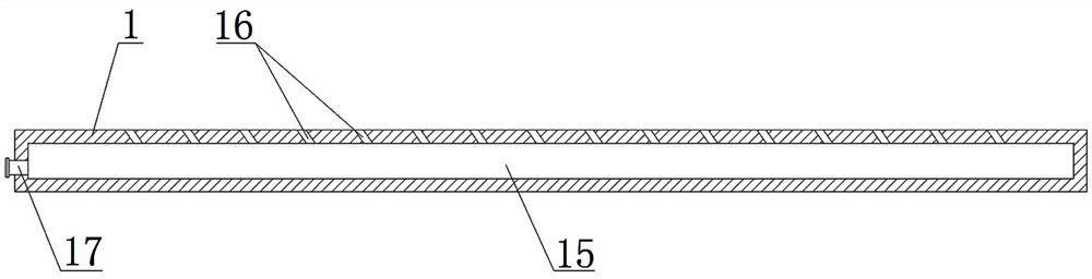
[0025] like Figure 1~4 As shown, a high-precision jig for tooling and positioning printed circuit boards includes a chassis 1, a left baffle 2 and a right baffle 3 are respectively welded on the top surface of the chassis 1 and on the left and right sides thereof, and the chassis 1 On the top surface of the top surface and at its front and rear ends, a front baffle 4 and a rear baffle 5 are respectively welded, and the front baffle 4 and the rear baffle 5 are all arranged between the left baffle 2 and the right baffle 3, and the front baffle 4 A heat conduction plate 6 is fixed between the rear baffle plate 5 and the front baffle plate 4 and the right baffle plate 3 are respectively provided with a front pressing mechanism and a right pressing mechanism, and the front pressing mechanism includes a ...


PUM


Abstract

The invention discloses a high-precision jig for tooling and positioning printed circuit boards, which includes a chassis (1), on the top surface of the chassis (1) and on the left and right sides thereof, a left baffle (2) and a Right baffle (3), front baffle (4) and rear baffle (5), front baffle (4) and right baffle (3) are welded respectively on the top surface of chassis (1) and at its front and rear ends A front pressing mechanism and a right pressing mechanism are respectively arranged on the top, a closed cavity (15) is opened in the chassis (1), and a plurality of oblique holes (16) connecting the closed cavity (15) are opened on the top surface of the chassis (1). ), the side wall of the chassis (1) is also provided with a joint (17) connected to the closed cavity (15), and the other end of the joint (17) is connected with a blower (18). The invention has the beneficial effects of improving the efficiency of the printed circuit board positioning tool, reducing the working intensity and improving the welding precision.

Description

technical field [0001] The invention relates to the technical field of a jig structure for fixing a printed circuit board, in particular to a high-precision jig for positioning a printed circuit board by a jig and a working method. Background technique [0002] When the printed circuit board is produced, the printed circuit board is usually placed on a carrier first, and then a solder paste layer is applied on the place where the electronic components need to be soldered on the printed circuit board, and then the leads of the electronic components are placed Place the pins on the solder paste, and finally use a soldering machine to solder the pins, so that the electronic components are soldered to the printed circuit board to achieve the fixing effect of the electrical connection. There is no structure for fixing the circuit board on the traditional jig, only a groove for the circuit board to be placed. After the printed circuit board is placed in the groove, it is necessary...

Claims


Application Information

Patent Timeline
Patent Type & Authority Patents(China)
IPC IPC(8): H05K3/34
CPCH05K3/34H05K2203/048
Inventor 李清华张仁军艾克华黄伟杰牟玉贵杨海军
Owner 四川英创力电子科技股份有限公司
Features
  • R&D
  • Intellectual Property
  • Life Sciences
  • Materials
  • Tech Scout
  • Unparalleled Data Quality
  • Higher Quality Content
  • 60% Fewer Hallucinations
Learn More