Silicon wafer positive photoresist etching equipment and process for power supply chip production

A photoresist and power chip technology, which is applied in the field of silicon wafer positive photoresist etching equipment and process for power chip production, can solve the problems of slow etching speed, waste of resist spray and the like

Pending Publication Date: 2021-05-18
薛俊治
View PDF0 Cites 0 Cited by
  • Summary
  • Abstract
  • Description
  • Claims
  • Application Information

AI Technical Summary

Problems solved by technology

[0005] Aiming at the deficiencies of the prior art, the present invention provides silicon wafer positive photoresist etching equipment for the production of power chips, which has the advantages of intermittent spraying of resist and heating of the resist, and solves the waste of resist spraying. and the problem of slow etching speed

Method used


Image

  • Silicon wafer positive photoresist etching equipment and process for power supply chip production
  • Silicon wafer positive photoresist etching equipment and process for power supply chip production
  • Silicon wafer positive photoresist etching equipment and process for power supply chip production

Examples


Embodiment Construction

[0034] The following will clearly and completely describe the technical solutions in the embodiments of the present invention with reference to the accompanying drawings in the embodiments of the present invention. Obviously, the described embodiments are only some, not all, embodiments of the present invention. Based on the embodiments of the present invention, all other embodiments obtained by persons of ordinary skill in the art without making creative efforts belong to the protection scope of the present invention.

[0035] As introduced in the background technology, there are deficiencies in the prior art. In order to solve the above technical problems, the application proposes silicon wafer positive photoresist etching equipment for power chip production

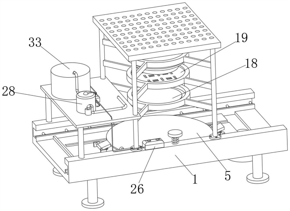
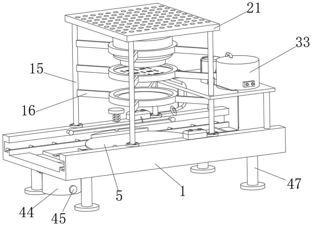
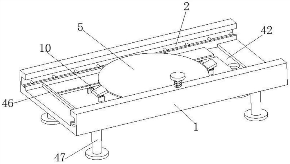
[0036] In a typical implementation of the present application, such as Figure 1-10 As shown, the silicon wafer positive photoresist etching equipment for power chip production includes an operating table 1, and the in...


PUM


Abstract

The invention relates to the technical field of silicon wafer preparation devices, and discloses silicon wafer positive photoresist etching equipment and process for power supply chip production, temperature detection can be carried out on a photoresist through arrangement of a temperature sensor, when the temperature is too low, a heating wire starts to heat the photoresist, and the activity of the photoresist is enhanced, so the sprayed-out photoresist is capable of increasing the speed of etching the silicon wafer. The two position indicators detect the silicon wafer, when the silicon wafer is detected, the position indicators transmit signals into the position processor through the conduction wires, the central controller starts the liquid pump through the intermittent wire, the liquid inlet pipe discharges the photoresist in the liquid storage tank into the liquid pump, the resist is squeezed out of the liquid pipe under the pressurization action of the liquid pump and finally sprayed on the silicon wafer through a porous spray head, and when the position indicators cannot detect the silicon wafer, the liquid pump stops working, so that intermittent spraying is realized, and waste of the resist caused by continuous spraying is prevented.

Description

technical field [0001] The invention relates to the technical field of silicon wafer preparation devices, in particular to silicon wafer positive photoresist etching equipment and technology for power chip production. Background technique [0002] The production of power chips includes the step of etching. The etching process is a key step in transferring the circuit layout to the chip, including etching and cleaning after etching. At this stage, the etching and cleaning technology required for multi-layer wires is the focus. Etching technology development has completed the 0.2-micron contact window etching technology that meets the 0.15-micron generation process specification and the aluminum wire etching technology that meets the 0.18-micron generation process specification (line width / space=0.22 micron / 0.23 micron); at the same time, the photoresist hardening technology has been completed. It can improve photoresist etching by 10% to 20%. The current technical focus is on...

Claims


Application Information

Patent Timeline
Patent Type & Authority Applications(China)
IPC IPC(8): G03F1/80H01L21/027H01L21/033
CPCG03F1/80H01L21/0273H01L21/0337
Inventor 苏日荣黄鑫
Owner 薛俊治
Why Eureka
Try Eureka