Chip packaging structure and assembling method thereof

A technology of chip packaging structure and assembly method, applied in electrical components, electrical solid devices, circuits, etc., can solve the problems of high voltage, easy to be interfered by strong electromagnetic fields, and unable to withstand high temperature.

Pending Publication Date: 2021-05-18
华远微电科技(深圳)有限公司
View PDF0 Cites 11 Cited by
  • Summary
  • Abstract
  • Description
  • Claims
  • Application Information

AI Technical Summary

Problems solved by technology

[0004] Aiming at the deficiencies of the prior art, the present invention provides a chip packaging structure and its assembly method, aiming to solve the problems that the existing chip packaging structure cannot withstand high temperature, high voltage and is easily disturbed by strong electromagnetic fields

Method used


Image

  • Chip packaging structure and assembling method thereof
  • Chip packaging structure and assembling method thereof

Examples


Embodiment Construction

[0036] In order to describe the technical content, structural features, achieved goals and effects of the present invention in detail, the following will be described in detail in conjunction with the embodiments and accompanying drawings.

[0037] Embodiments of the present invention are described in detail below, examples of which are shown in the drawings, wherein the same or similar reference numerals designate the same or similar elements or elements having the same or similar functions throughout. The embodiments described below by referring to the figures are exemplary and are intended to explain the present invention and should not be construed as limiting the present invention.

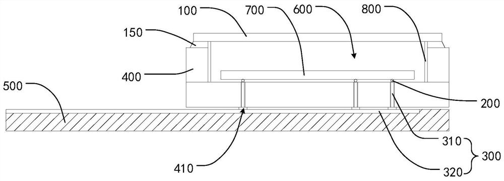
[0038] Please refer to figure 1 , figure 1 A cross-sectional view of a chip package structure provided by an embodiment of the present invention. Such as figure 1 As shown, a chip packaging structure includes a metal cover 100, a metal ball 200, a metal connector 300, a ceramic case 400 an...


PUM


Abstract

The invention provides a chip packaging structure and an assembling method thereof. The chip packaging structure comprises a metal cover plate, a metal ball, a metal connecting piece, a ceramic shell and a ceramic antenna, the metal cover plate is connected with the ceramic shell to form a closed cavity, the cavity is used for containing a chip, and the inner side wall of the ceramic shell is provided with a metal coating. The chip is welded on the inner bottom surface of the ceramic shell through the metal ball, and the metal connecting piece for connecting the metal ball and a ceramic antenna arranged on the outer bottom surface of the ceramic shell is embedded in the bottom of the ceramic shell. According to the invention, through the shielding effect of the metal cover plate and the metal coating, the chip can work normally in a strong electromagnetic interference environment, and through the arrangement of the ceramic shell and the ceramic antenna, the chip can carry out normal signal transmission in a high-temperature environment.

Description

technical field [0001] The invention relates to the technical field of chip packaging, in particular to a chip packaging structure and an assembly method thereof. Background technique [0002] When conducting inspections of power equipment, if manual inspections are performed according to the specified inspection cycle, the amount of inspections and recorded data will be huge. Therefore, temperature sensors are generally used to understand the temperature of each device in real time during operation. [0003] Traditional temperature sensor chip packaging structures generally have disadvantages such as poor sealing reliability, large size, no anti-electromagnetic interference function, and inability to withstand high temperatures. For the temperature detection of special key positions in some substations, such as high voltage switch contacts in high voltage, high temperature, strong magnetic field and extremely strong electromagnetic interference environment, in order to real...

Claims


Application Information

Patent Timeline
Patent Type & Authority Applications(China)
IPC IPC(8): H01L23/31H01L23/60H01L23/66H01L21/56
CPCH01L21/561H01L23/3121H01L23/60H01L23/66H01L2223/6677
Inventor 刘长顺刘兵余锐坤杨宗伟张志远李庭举卢翠马子轩姜琳
Owner 华远微电科技(深圳)有限公司
Why Eureka
Try Eureka