Semiconductor structure and manufacturing method thereof

A manufacturing method and semiconductor technology, applied in the fields of semiconductor/solid-state device manufacturing, semiconductor devices, semiconductor/solid-state device components, etc., can solve the problems of product performance impact, easy oxidation of conductive pillars, etc., and shorten the manufacturing cycle and process time. , to avoid the effect of air voids

Inactive Publication Date: 2021-06-01
CHANGXIN MEMORY TECH INC
View PDF6 Cites 0 Cited by
  • Summary
  • Abstract
  • Description
  • Claims
  • Application Information

AI Technical Summary

Problems solved by technology

Due to the characteristics of the conductive pillars being easily oxidized, it has an impact on the performance of the product

Method used


Image

  • Semiconductor structure and manufacturing method thereof
  • Semiconductor structure and manufacturing method thereof
  • Semiconductor structure and manufacturing method thereof

Examples


Embodiment Construction

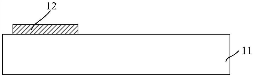
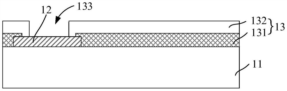
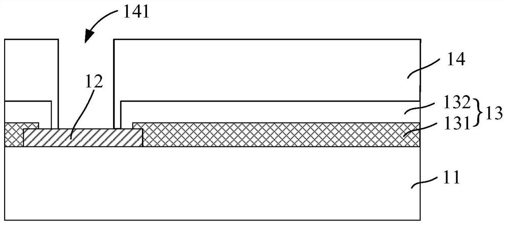
[0020] It can be seen from the background art that there is a need to provide a semiconductor structure and a manufacturing method thereof, and the semiconductor structure manufacturing method can manufacture a semiconductor structure with oxidation resistance.

[0021] In order to solve the above technical problems, an embodiment of the present invention provides a method for manufacturing a semiconductor structure, which melts the second conductive layer formed on the first conductive layer through a reflow process, so that the second conductive layer simultaneously covers the side of the first conductive layer The walls and top, in this way, help to reduce process steps and shorten the manufacturing cycle.

[0022] In order to make the purpose, technical solutions and advantages of the embodiments of the present invention clearer, the embodiments of the present invention will be described in detail below with reference to the accompanying drawings. However, those skilled in...


PUM

PropertyMeasurementUnit
thicknessaaaaaaaaaa
thicknessaaaaaaaaaa
thicknessaaaaaaaaaa

Abstract

The embodiment of the invention relates to a semiconductor structure and a manufacturing method thereof. The manufacturing method of the semiconductor structure comprises the steps of providing a substrate and a welding pad located on the substrate, forming an insulating medium layer on the substrate, wherein the insulating medium layer covers the welding pad, patterning the insulating dielectric layer, forming a first window in the insulating dielectric layer, and enabling the first window to expose the welding pad, forming a mask layer is formed on the insulating dielectric layer, the mask layer is patterned, a second window is formed in the first window, and the welding pad is exposed out of the second window; forming a first conductive layer in the second window, forming a second conductive layer on the first conductive layer, removing the mask layer to expose the side wall of the first conductive layer, and performing reflow treatment on the second conductive layer, so that the second conductive layer covers the top and the side wall of the first conductive layer at the same time. The reflow treatment process is adopted, the second conductive layers located on the top and the side wall of the first conductive layer are integrally formed, and connecting gaps are eliminated.

Description

technical field [0001] The invention relates to the field of semiconductor manufacturing, in particular to a semiconductor structure and a manufacturing method thereof. Background technique [0002] With the development of the chip manufacturing process, the pillar bump technology has gradually become the mainstream technology, and the connection between the chip and the substrate is realized through the pillar bump technology. The existing pillar bump is usually composed of a conductive pillar and a solder cap. Due to the characteristics of the conductive pillars being easily oxidized, the performance of the product has been affected. Especially as the chip density is getting higher and higher, the distance between chips is decreasing, and the size of the stud bump is also gradually reduced. How to effectively protect the surface of the stud bump is particularly important. Contents of the invention [0003] Embodiments of the present invention provide a semiconductor str...

Claims


Application Information

Patent Timeline
Patent Type & Authority Applications(China)
IPC IPC(8): H01L23/488H01L21/48
CPCH01L24/10H01L24/12H01L24/16H01L24/11
Inventor 范增焰
Owner CHANGXIN MEMORY TECH INC
Why Eureka
Try Eureka