Cutting forming method of wafer-level laminated plastic package wafer
A molding method, wafer-level technology, applied in electrical components, semiconductor/solid-state device manufacturing, circuits, etc., can solve problems such as deformation and impact on bump production
- Summary
- Abstract
- Description
- Claims
- Application Information
AI Technical Summary
Problems solved by technology
Method used
Image
Examples
Embodiment
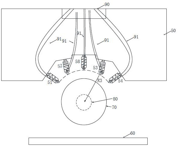
[0068] The cutting platform of a kind of wafer-level laminated plastic-encapsulated wafer of the present invention, as Figure 2 to Figure 4 As shown, it includes a cutting knife set 50 , a chassis 70 , a rotating motor 80 and a film waste suction system 90 , and the chassis 70 sucks the molded wafer 20 by vacuum. The rotating motor 80 drives the chassis 70 of the cutting platform to rotate clockwise or counterclockwise.
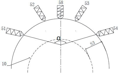
[0069] The cutter group 50 is arranged on one side of the chassis 70, and it arranges the cutter I51, the cutter II52, the file 58, the cutter III53 and the cutter IV54 sequentially from left to right, the cutter II52, the cutter III53 The file 58 is symmetrical to the center line, and the cutter I 51 and IV 54 are also symmetrical to the file 58; Arranged in an arc shape, an arc is formed around the chassis 70, and the radius of the arc is R3.
[0070] The included angle α between the cutting knife I51 and the cutting knife IV54 is in the range of 90°≤α≤1...
PUM
 Abstract
Description
Claims
Application Information


