Method for trimming MOSFET device layout

A layout and device technology, which is applied in the field of MOSFET device layout trimming, can solve problems such as heavy workload, increasing the size of MOSFET device layout graphics, and affecting the size of MOSFET devices.

Pending Publication Date: 2021-06-08
SHANGHAI HUAHONG GRACE SEMICON MFG CORP
View PDF0 Cites 3 Cited by
  • Summary
  • Abstract
  • Description
  • Claims
  • Application Information

AI Technical Summary

Problems solved by technology

In the prior art, when trimming the layout of the MOSFET device, the entire layout of the layout of the MOSFET device (graphic arrangement, size and shape in the layout), etc., will be modified, that is, a large number of modifications are required to the layout of the MOSFET device. On the one hand The corresponding workload is very large. On the other hand, after modifying the entire layout of the MOSFET device layout, the graphic size in the MOSFET device layout may be increased, which will affect the size of the formed MOSFET device. Therefore, a new MOSFET device is required Layout trimming method to complete layout modification simply and quickly, and realize power consumption optimization at the layout design level

Method used


Image

  • Method for trimming MOSFET device layout
  • Method for trimming MOSFET device layout
  • Method for trimming MOSFET device layout

Examples


Embodiment Construction

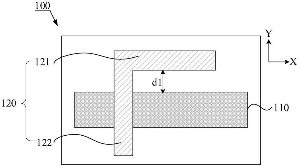
[0036] The method for trimming the layout of the MOSFET device proposed by the present invention will be further described in detail below in conjunction with the accompanying drawings and specific embodiments. The advantages and features of the present invention will become clearer from the following description. It should be noted that all the drawings are in a very simplified form and use imprecise scales, and are only used to facilitate and clearly assist the purpose of illustrating the embodiments of the present invention.

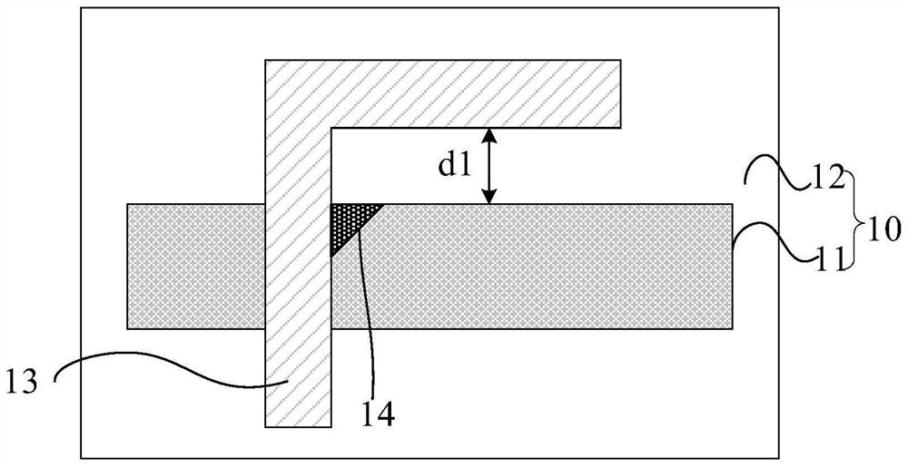
[0037]The inventors found that the reason for the shaded area in the active region of the existing MOSFET device is that the distance between the active region pattern and the first floating gate sub-pattern in the original layout of the MOSFET device is relatively small, resulting in In the manufacturing process corresponding to the layout of the active region and the layout of the floating gate, the distance between the floating gate corresponding t...


PUM


Abstract

The invention provides a method for trimming an MOSFET device layout, which comprises the following steps of: acquiring an original layout, and modifying a design rule of the original layout; and then modifying a floating gate layout according to the modified design rule of the original layout, and reducing the sizes of all floating gate patterns in the floating gate layout so as to increase the distance between a first floating gate sub-pattern and an active region pattern. In this way, modification of the original layout can be completed simply and quickly, and power consumption optimization on the layout design level is achieved.

Description

technical field [0001] The invention relates to the technical field of semiconductor manufacturing, in particular to a method for trimming the layout of a MOSFET device. Background technique [0002] In the prior art, the MOSFET device (Metal-Oxide-Semiconductor Field-Effect Transistor, Metal-Oxide-Semiconductor Field-Effect Transistor) layout (Layout) includes the size of the MOSFET device and the relevant physical information data of each process layer in the MOSFET device, It is a bridge for MOSFET devices from design to manufacture. Such as figure 1 as shown, figure 1 is a schematic diagram of the structure formed in the manufacturing method of the MOSFET device in the prior art. The manufacturing method of existing MOSFET device generally comprises: provide semiconductor substrate 10, described semiconductor substrate 10 comprises active region 11 and isolation region 12, forms floating gate 13 on described active region, and described floating gate 13 Covering part...

Claims


Application Information

Patent Timeline
Patent Type & Authority Applications(China)
IPC IPC(8): H01L29/66H01L29/40H01L21/027H01L29/423
CPCH01L29/66477H01L29/401H01L21/027H01L29/42324
Inventor 孙访策郑舒静林晓帆黄冲张明
Owner SHANGHAI HUAHONG GRACE SEMICON MFG CORP
Why Eureka
Try Eureka