Automatic wiring method and device of chip top layer long and narrow channel and storage medium

An automatic wiring, narrow and long channel technology, applied in special data processing applications, instruments, electrical digital data processing and other directions, can solve problems such as winding congestion, and achieve the effect of solving local winding congestion and alleviating insufficient winding resources.

Pending Publication Date: 2021-06-11
广芯微电子(广州)股份有限公司
View PDF9 Cites 0 Cited by
  • Summary
  • Abstract
  • Description
  • Claims
  • Application Information

AI Technical Summary

Problems solved by technology

[0004] The embodiment of the present invention provides an automatic wiring method, device and storage medium for the narrow and long channel on the top layer of the chip, which can solve the problem of winding congestion in the prior art when the narrow and long channel is automatically routed

Method used


Image

  • Automatic wiring method and device of chip top layer long and narrow channel and storage medium
  • Automatic wiring method and device of chip top layer long and narrow channel and storage medium
  • Automatic wiring method and device of chip top layer long and narrow channel and storage medium

Examples


Embodiment Construction

[0038] The following will clearly and completely describe the technical solutions in the embodiments of the present invention with reference to the accompanying drawings in the embodiments of the present invention. Obviously, the described embodiments are only some, not all, embodiments of the present invention. Based on the embodiments of the present invention, all other embodiments obtained by persons of ordinary skill in the art without creative efforts fall within the protection scope of the present invention.

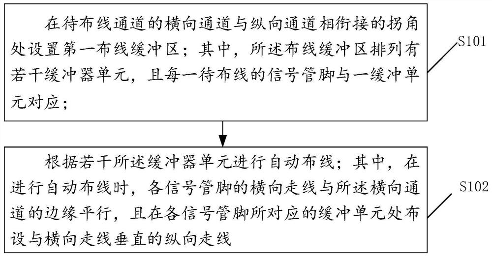
[0039] Such as figure 2 As shown, an embodiment of the present invention provides a method for automatic routing of long and narrow channels on the top layer of a chip, including:

[0040] Step S101: Set a first wiring buffer at the corner where the horizontal channel and the vertical channel of the channel to be wired are connected; wherein, the wiring buffer is arranged with a number of buffer units, and each signal pin to be wired is connected to a The buffer ...


PUM


Abstract

The invention discloses an automatic wiring method and device for a chip top layer long and narrow channel and a storage medium. The method comprises the steps: arranging a first wiring buffer area at the corner where a transverse channel and a longitudinal channel of a channel to be wired are connected, wherein a plurality of buffer units are arranged in the wiring buffer area, and each signal pin to be wired corresponds to one buffer unit; performing automatic wiring according to the plurality of buffer units, wherein during automatic wiring, transverse wires of all the signal pins are parallel to the edge of the transverse channel, and longitudinal wires perpendicular to the transverse wires are arranged at the positions, corresponding to the signal pins, of the buffer units. By implementing the embodiment of the invention, the problem of winding congestion during automatic wiring in a long and narrow channel in the prior art can be solved.

Description

technical field [0001] The invention relates to the technical field of chip design, in particular to an automatic wiring method, device and storage medium for a long and narrow channel on the top layer of a chip. Background technique [0002] With the further expansion of the scale of integrated circuits and the gradual reduction of the size of process nodes, more and more chips will adopt multi-level implementation methods in the physical implementation stage. The common ones are two-layer or three-layer design structures. The advantages of multi-level design structures Modules at all levels are implemented in parallel, so as to improve the implementation efficiency of the chip physical design stage. When dividing the multi-level structure, it is necessary to consider the logical size, functional complexity and physical realizability of the individual modules to be divided. The highest level is also called the top level. The top level generally retains the chip input and o...

Claims


Application Information

Patent Timeline
IPC IPC(8): G06F30/394
CPCG06F30/394
Inventor 王锐关娜王亚波李建军莫军
Owner 广芯微电子(广州)股份有限公司
Why Eureka
Try Eureka