Electronic device and its manufacturing method

A technology of electronic devices and components, which is applied in the field of electronic devices and their preparation, can solve problems such as poor vacuum in sealed chambers, and achieve the effect of reducing the difficulty of peeling and improving quality

Active Publication Date: 2021-08-13
SEMICON MFG ELECTRONICS (SHAOXING) CORP
View PDF0 Cites 0 Cited by
  • Summary
  • Abstract
  • Description
  • Claims
  • Application Information

AI Technical Summary

Problems solved by technology

[0004] However, the electronic device with a sealed cavity prepared based on the existing technology still has the problem of poor vacuum in the sealed cavity.

Method used


Image

  • Electronic device and its manufacturing method
  • Electronic device and its manufacturing method
  • Electronic device and its manufacturing method

Examples


preparation example Construction

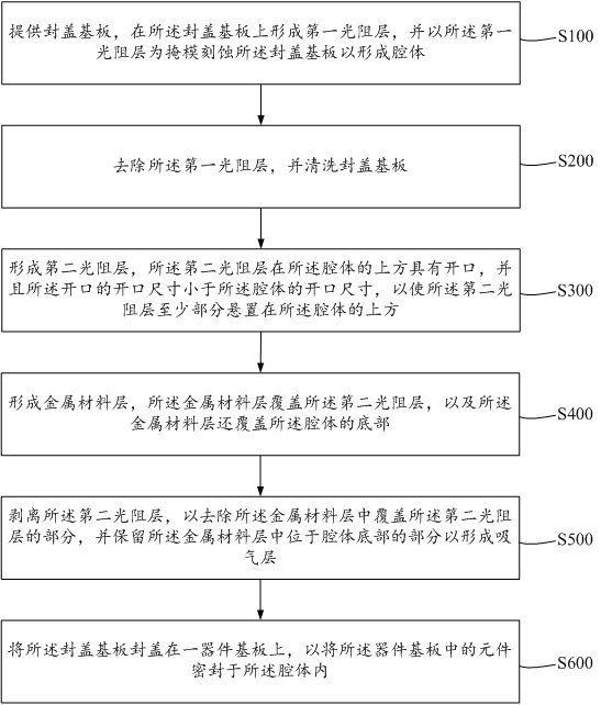
[0026] Therefore, the present invention provides a method for preparing an electronic device, so as to increase the vacuum degree of the formed sealed cavity and ensure the quality of the prepared gettering layer. Specifically, the preparation method of the electronic device provided by the present invention can refer to image 3 , which includes the following steps.

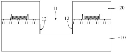
[0027] Step S100 , providing a first substrate, forming a first photoresist layer on the first substrate, and etching the first substrate using the first photoresist layer as a mask to form a cavity.

[0028] Step S200 , removing the first photoresist layer, and wet cleaning the first substrate.

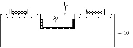
[0029] Step S300, forming a second photoresist layer on the first substrate, the second photoresist layer has an opening above the cavity, and the opening size of the opening is smaller than the opening size of the cavity, The part of the second photoresist layer located in the cavity is suspended relative to the bot...


PUM


Abstract

The invention provides an electronic device and a preparation method thereof. After the cavity is formed by etching, the first photoresist layer can be removed, thereby allowing the first substrate to be cleaned, preventing the polymer residue generated after etching from affecting the vacuum of the sealed cavity, and preparing the second substrate. The topography of the second photoresist layer can be more flexibly adjusted during the photoresist layer, so as to further reduce the difficulty of stripping the second photoresist layer in the stripping process, and help improve the quality of the finally formed getter layer.

Description

technical field [0001] The invention relates to the technical field of semiconductors, in particular to an electronic device and a preparation method thereof. Background technique [0002] Among widely used electronic devices, some devices need to work normally in an ideal vacuum environment, such as electronic devices with micro-electro-mechanical systems (Micro-Electro-Mechanical Systems, MEMS). [0003] Such electronic devices usually use a sealed cavity to provide a vacuum environment for the electronic components, so that the electronic components in the sealed cavity can work in a high vacuum environment. Taking an electronic device with a MEMS element as an example, the MEMS element is arranged in a sealed cavity accordingly, so as to ensure that the micro-mechanical structure therein has excellent vibration performance and improve its reliability. In addition, in order to further improve the vacuum performance of the sealed cavity, a metal layer is generally formed ...

Claims


Application Information

Patent Timeline
Patent Type & Authority Patents(China)
IPC IPC(8): B81C1/00B81B7/00
CPCB81B7/0038B81C1/00047B81C1/00285
Inventor 吕林静许继辉
Owner SEMICON MFG ELECTRONICS (SHAOXING) CORP
Why Eureka
Try Eureka