Supercharge Your Innovation With Domain-Expert AI Agents!

Beam guide wiring structure, optical scanning device and calibration method thereof

An optical scanning device and a wiring structure technology, applied in the fields of optical scanning device and its calibration, beam guiding wiring structure, can solve problems such as optical signal crosstalk, and achieve the effects of optimizing spacing, eliminating grating lobes and eliminating crosstalk phenomenon

Pending Publication Date: 2021-06-18
长沙思木锐信息技术有限公司
View PDF0 Cites 3 Cited by
  • Summary
  • Abstract
  • Description
  • Claims
  • Application Information

AI Technical Summary

Problems solved by technology

Although the dense wiring structure has many advantages, when the optical signal transmission is realized through parallel waveguides / transmission lines in the existing dense wiring structure, crosstalk between the optical signals transmitted between the waveguides usually occurs

Method used


Image

  • Beam guide wiring structure, optical scanning device and calibration method thereof
  • Beam guide wiring structure, optical scanning device and calibration method thereof
  • Beam guide wiring structure, optical scanning device and calibration method thereof

Examples


Embodiment Construction

[0046] The following will clearly and completely describe the technical solutions in the embodiments of the present invention with reference to the accompanying drawings in the embodiments of the present invention. Obviously, the described embodiments are only some, not all, embodiments of the present invention. Based on the embodiments of the present invention, all other embodiments obtained by persons of ordinary skill in the art without making creative efforts belong to the protection scope of the present invention.

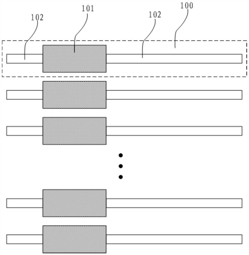
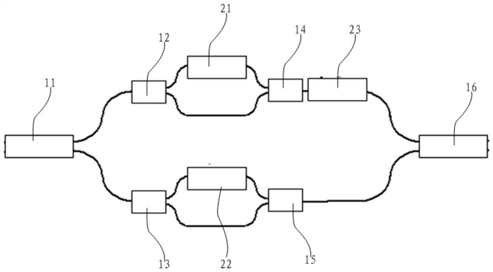
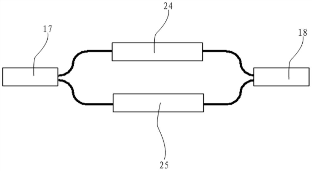
[0047]As mentioned in the background technology, in many applications, multiple sets of dense parallel waveguides / transmission lines are required to realize optical signal transmission. The dense waveguide wiring structure can save chip area and increase chip integration, which can be used for two-dimensional microwave / millimeter wave radar Traces. More importantly, in the optical phased array, the dense waveguide wiring structure can eliminate grating lobes. ...


PUM


Abstract

The invention provides a beam guide wiring structure, an optical scanning device and a calibration method thereof, which can achieve the purpose of eliminating grating lobes by optimizing the distance between adjacent beam guide branches, but can introduce crosstalk between waveguides. The structure comprises a plurality of beam guiding branches, each beam guiding branch is connected with an input light beam, and phase and intensity modulation is performed on the input light beams through a phase and intensity modulator, so that one of the plurality of beam guiding branches outputs a scanning light beam with a preset phase, preset intensity and a preset scanning direction. Or each beam guiding branch outputs a scanning beam with a corresponding preset phase, preset intensity and preset scanning direction, so that a single-point triggering beam guiding mode and an optical phased array mode are realized. According to the invention, phase and intensity adjustment is carried out on the optical signals of the beam guiding branches through the phase and intensity modulator, so that deviation caused by crosstalk is compensated, and the purpose of eliminating the crosstalk phenomenon of the optical signals between the beam guiding branches is achieved.

Description

technical field [0001] The present invention relates to the technical field of laser radar, and more specifically, relates to a beam guiding wiring structure, an optical scanning device and a calibration method thereof. Background technique [0002] In many applications, multiple sets of dense parallel waveguides / transmission lines are required to realize optical signal transmission. The dense waveguide wiring structure can save chip area and increase chip integration. It can be used for two-dimensional microwave / millimeter wave radar wiring. More importantly, in the optical phased array, the dense waveguide wiring structure can eliminate grating lobes. Although the dense wiring structure has many advantages, when the optical signal transmission is implemented through parallel waveguides / transmission lines in the existing dense wiring structure, crosstalk of the optical signals transmitted between the waveguides usually occurs. Contents of the invention [0003] In view o...

Claims


Application Information

Patent Timeline
Patent Type & Authority Applications(China)
IPC IPC(8): G01S7/481G01S7/483G01S7/497G01S17/89
CPCG01S7/481G01S7/483G01S7/497G01S17/89
Inventor 张璟
Owner 长沙思木锐信息技术有限公司
Features
  • R&D
  • Intellectual Property
  • Life Sciences
  • Materials
  • Tech Scout
  • Unparalleled Data Quality
  • Higher Quality Content
  • 60% Fewer Hallucinations
Learn More