
FPGA-based I3C logic controller implementation method, I3C read-write test device and I3C read-write test system

A technology of logic controller and implementation method, applied in general control system, control/regulation system, program control, etc., can solve problems such as inability to test camera modules

Active Publication Date: 2021-06-25
SHENZHEN DOTHINKEY TECH
View PDF5 Cites 0 Cited by
  • Summary
  • Abstract
  • Description
  • Claims
  • Application Information

AI Technical Summary

Problems solved by technology

[0004] This application provides a FPGA-based I3C logic controller implementation method, I3C reading and writing test device and system, which are used to overcome the technical defect that existing processors cannot test camera modules with I3C bus interfaces, and provide a method based on The I3C logic controller of FPGA and its implementation method realize the testing of the camera module with I3C bus interface

Method used


Image

  • FPGA-based I3C logic controller implementation method, I3C read-write test device and I3C read-write test system
  • FPGA-based I3C logic controller implementation method, I3C read-write test device and I3C read-write test system

Examples


Embodiment 1

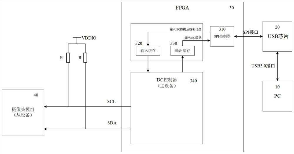
[0071] Such as figure 1 As shown, the present application provides a kind of I3C reading and writing test system, including PC upper computer 10, USB chip 20, FPGA30, I3C slave device (here is camera module) 40; USB module 20 is connected with upper computer 10 through USB line , used to transmit data between host computer 10 and USB chip 20; USB chip 20 is connected to FPGA 30 through SPI bus, used for data transmission between USB chip 20 (USB3.0 chip is used in this solution) and FPGA 30, FPGA 30 The SPI controller 310 is implemented by FPGA internal logic. The USB chip 20 is connected to the PC host computer 10 through a USB bus.

[0072] The SPI controller 310 receives the control command sent from the PC host computer 10 and writes it into the input buffer 320; the control information includes a start signal, an end signal, a master device waiting for a slave device response flag signal, a write data flag signal, and a read data flag signal. Flag signal, read data stop...

Embodiment 2

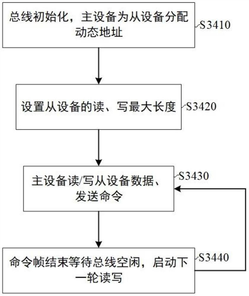
[0078] On the basis of Embodiment 1, this embodiment provides a method for implementing an FPGA-based I3C logic controller, including:

[0079] S100, receiving a control command output by the host computer based on the encapsulated I3C protocol;

[0080] Based on the user's operation instructions, the upper computer sends control instructions to the I3C main device FPGA30 according to the packaged I3C protocol, and writes the I3C read / write control commands and data into the FPGA internal input buffer through the USB3.0 interface and the SPI interface of the USB chip.

[0081] S200, assigning a dynamic address to a slave device with an I3C read / write function according to the control instruction, and setting a maximum length value of data that can be read / written once;

[0082] Based on the I3C control command of the upper computer, the I3C master device FPGA assigns a dynamic address (Dynamic Address) to the slave device with I3C read and write functions; the I3C bus includes...


PUM


Abstract

The invention discloses an FPGA-based I3C logic controller implementation method, an I3C read-write test device and an I3C read-write test system. The method comprises the following steps: receiving a control instruction output by an upper computer based on a packaged I3C protocol; according to the control instruction, distributing a dynamic address to the slave device with the I3C reading / writing function, and setting the maximum length value of one-time readable / writable data; sending an I3C read / write control command to the slave device based on a control instruction of the upper computer to realize an I3C read / write operation on the slave device; and sending the read slave device data or a write operation completion signal to an upper computer, and completing the I3C read / write control command. The method, the device and the system are used for solving the problem that a processor in the prior art does not support an I3C read-write function, and I3C data read-write and test are carried out on a camera module with an I3C bus interface.

Description

technical field [0001] The invention relates to the technical field of camera module testing, in particular to an FPGA-based I3C logic controller implementation method, I3C read-write test device and system. Background technique [0002] As mobile phone camera modules have higher and higher communication rate requirements, the original I2C communication bus rate is generally 100Kbps and 400Kbps, and a small number of I2C devices support 3.4Mbps, which cannot meet the needs of some high-end camera modules. The SPI communication bus Although the speed can be satisfied, the number of bus pins is large, which will undoubtedly increase the size of the mobile phone camera module. According to these requirements, the MIPI Alliance launched the I3C communication bus for mobile phone camera modules. Its advantages are that it can be backward compatible with I2C devices and has a high communication rate. Its SDR mode can support up to 12.5Mbps. The number of pins is the same as that o...

Claims


Application Information

Patent Timeline
Patent Type & Authority Applications(China)
IPC IPC(8): G05B19/042
CPCG05B19/0423G05B2219/21063Y02P90/02
Inventor 聂忠强李万泉
Owner SHENZHEN DOTHINKEY TECH
Features
  • Generate Ideas
  • Intellectual Property
  • Life Sciences
  • Materials
  • Tech Scout
  • Unparalleled Data Quality
  • Higher Quality Content
  • 60% Fewer Hallucinations
Learn More