Color spot repairing method of liquid crystal panel, system test architecture and DE-MURA equipment

A liquid crystal panel and repair method technology, applied in the direction of instruments, static indicators, etc., can solve the problems of high cost of low-standard products, loss of profits, occupation of color spots and elimination of production capacity, etc., to achieve the effect of increasing production capacity and reducing material costs

Pending Publication Date: 2021-06-25
深圳市联测光电科技有限公司
View PDF6 Cites 0 Cited by
  • Summary
  • Abstract
  • Description
  • Claims
  • Application Information

AI Technical Summary

Problems solved by technology

[0004] In the existing De-mura manufacturing process, there is no judgment on whether to remove the color spots on the panel first, resulting in the fact that the quality of the panel does not need to be removed, occupying the production capacity of the color spot removal, and virtually increasing the cost of the panel process
If the production line uses automatic pinning to supply power and drive signals to the PCBA test points, because the PCBA board is narrow, it is not easy to fix, and the copper on the PCBA board will be oxidized, resulting in poor contact, and the pinning block often deviates, resulting in poor display and video Incorrect interception, resulting in demura failure, low

Method used


Image

  • Color spot repairing method of liquid crystal panel, system test architecture and DE-MURA equipment
  • Color spot repairing method of liquid crystal panel, system test architecture and DE-MURA equipment
  • Color spot repairing method of liquid crystal panel, system test architecture and DE-MURA equipment

Examples


Embodiment Construction

[0061] The following will clearly and completely describe the technical solutions in the embodiments of the present invention with reference to the accompanying drawings in the embodiments of the present invention. Obviously, the described embodiments are only some, not all, embodiments of the present invention. Based on the embodiments of the present invention, all other embodiments obtained by persons of ordinary skill in the art without making creative efforts belong to the protection scope of the present invention.

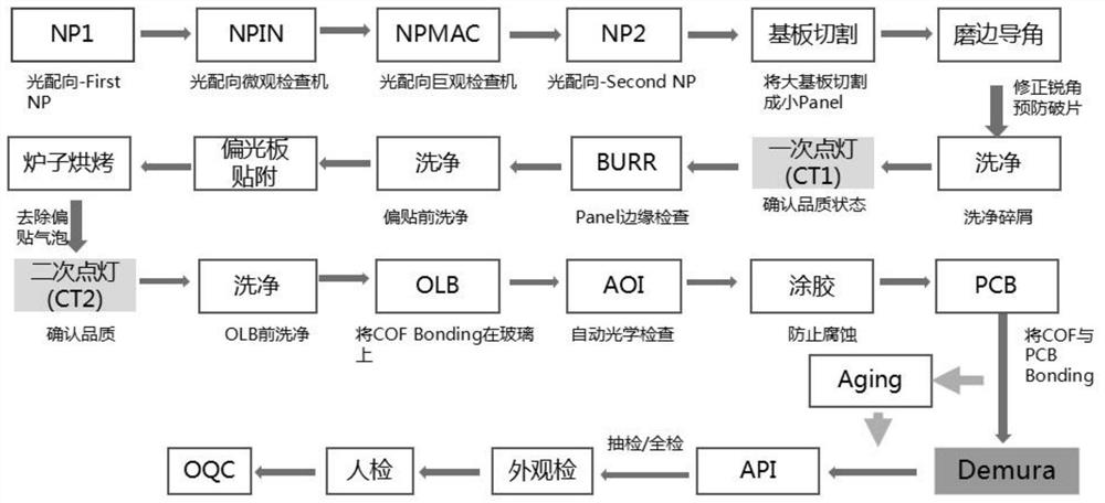
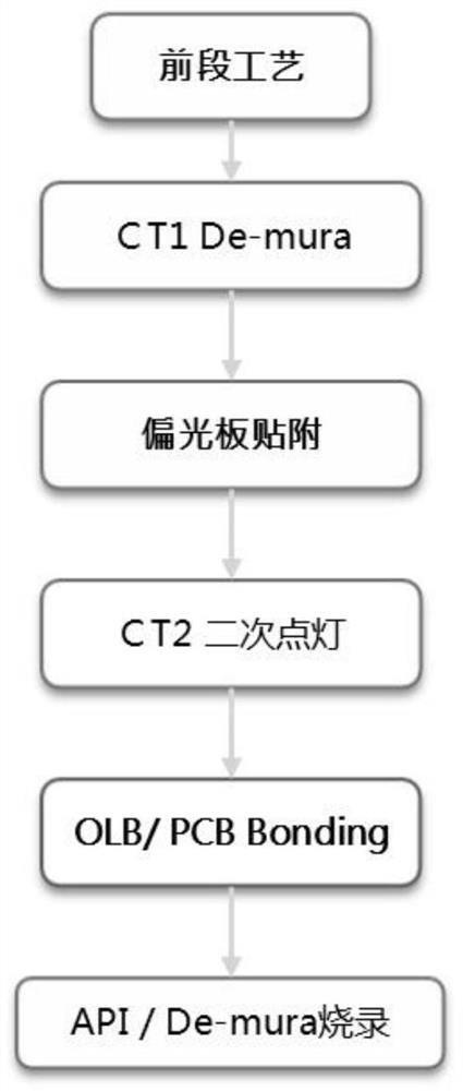
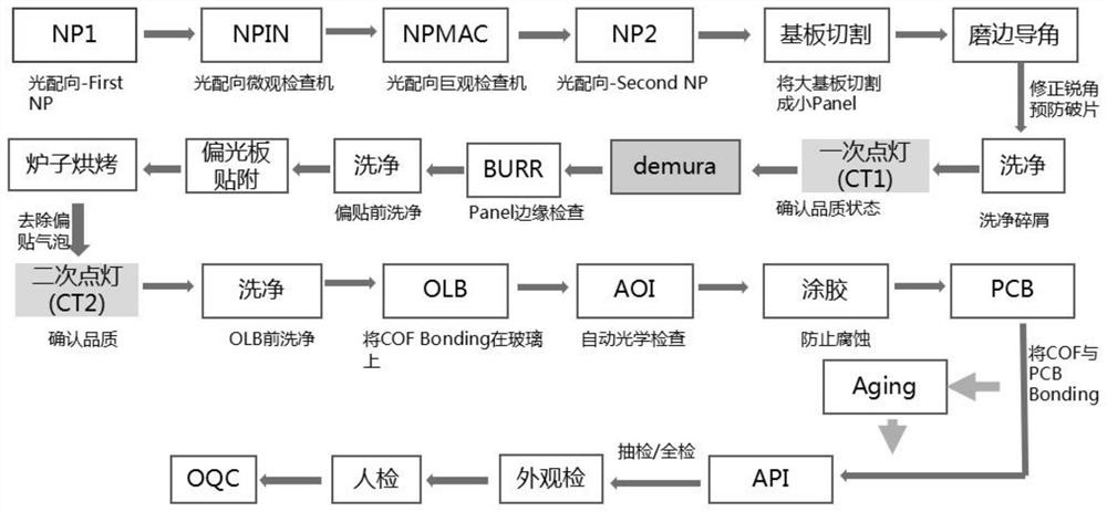
[0062] In order to overcome the shortcomings of the existing De-mura process, the present invention proposes a method for repairing color spots of a new liquid crystal panel, which is used to directly judge and repair the color spot defects of the panel after a lighting inspection of CT1. The method includes the following steps ;

[0063] In a lighting inspection, CT1 uses the image acquisition unit to judge the brightness uniformity of the panel, determine wh...


PUM


Abstract

The invention discloses a color spot repairing method for a liquid crystal panel, and the method is used for directly judging color spot defects of the panel and obtaining a repairing value after one-time lighting inspection (CT1), and comprises the following steps: adding an image acquisition unit to judge the brightness uniformity condition of a panel during one-time lighting inspection (CT1), determining whether the panel needs to be subjected to color spot defect repair (De-mura), performing De-mura processing on the panel which needs to be subjected to De-mura, and obtaining a repair value; and sequentially carrying out polaroid attachment and secondary lighting reinspection (CT2) on the panel. According to the method, the De-mura is moved to a one-time lighting inspection station to be processed, and the problem that the yield is low when a circuit PCBA board uses a test point to conduct needle insertion to make the De-mura is solved. Meanwhile, by determining whether the panel needs to be subjected to De-mura or not, De-mura processing is carried out on the panel needing to be subjected to De-mura; mass-production materials for normal panels and low-cost materials for low-specification panels can be distinguished, so the material cost is greatly reduced, and a polaroid, a driving chip and a circuit board can be saved.

Description

technical field [0001] The present invention relates to the technical field of liquid crystal displays, and more specifically relates to a method for repairing stains of liquid crystal panels, a system test framework and DE-MURA equipment used therein. Background technique [0002] In recent years, with the upgrading of domestic LCD panel lines, the shipment size of LCD panels has become larger and higher, and the resolution has become higher and higher. However, due to the complexity of the panel manufacturing process, the production speed has continued to increase, and the panel uniformity has become worse and worse. Yields are also decreasing. The De-mura automatic debugging system uses industrial cameras to sample gray-scale images, calculate algorithms, and obtain compensation data, which is used in De-mura IP to improve the uniformity of the panel. [0003] At present, the existing De-mura process is performed after PCBA bonding (that is, after COF and XB bonding). Fo...

Claims


Application Information

Patent Timeline
IPC IPC(8): G09G3/00G09G3/36
CPCG09G3/006G09G3/36
Inventor 黄浩
Owner 深圳市联测光电科技有限公司
Why Eureka
Try Eureka