Image calibration device and method for mark on printed board

A technology of printed board and calibration method, which is applied in the direction of assembling printed circuits with electrical components, and can solve the problem of inaccurate calibration of mark points or positioning base points, and the inability of circuit boards to accurately measure the distance between mark points or positioning base points and both sides, High labor costs and other issues

Active Publication Date: 2021-07-06
HONGYI TECH AUTOMATION EQUIP HUIZHOU CO LTD
View PDF7 Cites 4 Cited by
  • Summary
  • Abstract
  • Description
  • Claims
  • Application Information

AI Technical Summary

Problems solved by technology

[0003] During the board loading process, it is necessary to calibrate the mark point and the positioning base point of the circuit board. The calibration mark point is used to correspond to the stencil printing solder paste. The calibration positioning base point can be It is used to place thimble pins to fix the circuit board at a fixed point. After the circuit board is produced, it is necessary to identify and detect the two-dimensional code or barcode or other image marks. Traditionally, the mark point and the positioning base point are manually measured with a vernier caliper. Mark point or Position the distance between the base point and the two sides, and then input it into the control system and save it as the coordinate parameter. For regular circuit boards, it is impossible to determine its bou

Method used


Image

  • Image calibration device and method for mark on printed board
  • Image calibration device and method for mark on printed board
  • Image calibration device and method for mark on printed board

Examples


Embodiment Construction

[0040] In order to enable those skilled in the art to better understand the technical solution of the present invention, the product of the present invention will be further described in detail below in conjunction with the embodiments and accompanying drawings.

[0041] It should be noted that when an element is said to be "fixed" to another element, it can be directly on the other element or there can be an intervening element; when an element is said to be "connected" to another element, it can be A direct connection to another element or possibly an intervening element at the same time. The terms "vertical", "horizontal", "left", "right" and similar expressions are used herein for the purpose of description only and do not represent the only embodiment.

[0042] Unless otherwise defined, all technical and scientific terms used herein have the same meaning as commonly understood by one of ordinary skill in the technical field of the invention. The terminology used herein i...


PUM


Abstract

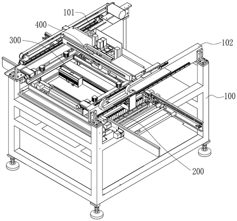
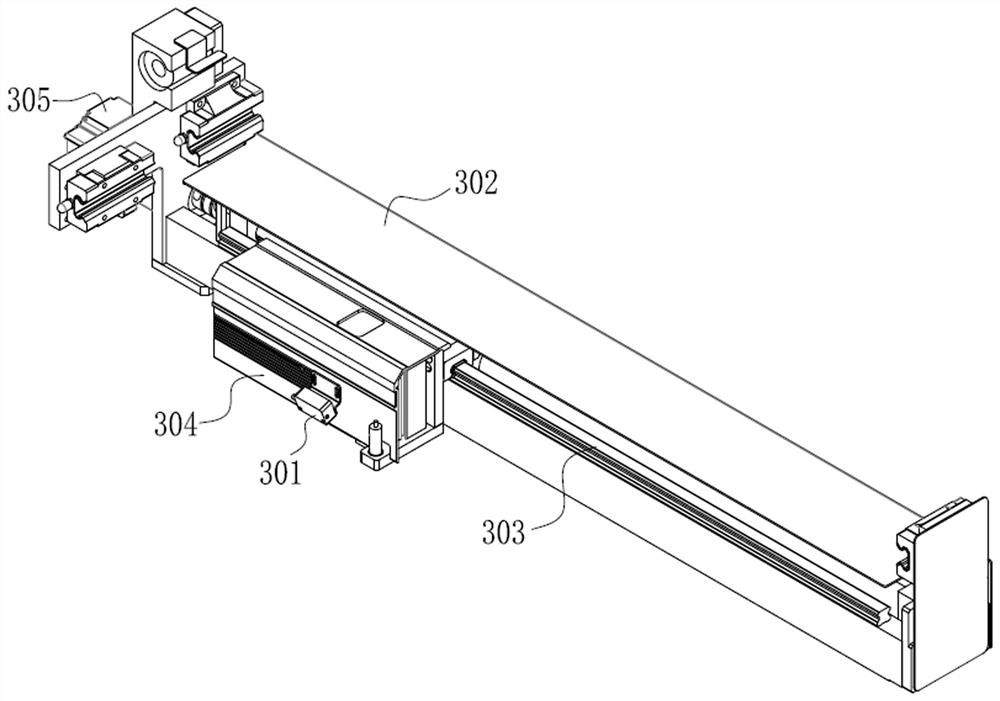
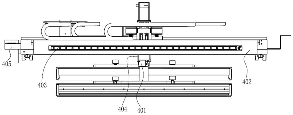
The invention discloses an image calibration device and method for a mark on a printed board, the image calibration device for the mark on the printed board comprises a board feeding unit, a main camera unit, an auxiliary camera unit and a control system, and the image calibration method for the mark on the printed board comprises the following steps: fixing and conveying the printed board by the board feeding unit; the auxiliary camera unit preliminarily shoots a printing plate image, uploads the image to a control system display screen, clicks to determine an image where the mark position is located, then the main camera unit converts the determined position image of the mark into a view, fine adjustment of mark coordinates is carried out, and after the mark position is fine adjusted, clicks, stores and establishes coordinate parameters of the mark, and the mark is calibrated; and then the control system controls the main camera unit to be converted into a view mode, the mark on the printed board is calibrated or scanned and recognized, and the calibration, calibration or detection work of the mark can be completed after calibration or scanning is completed. The calibration method is irrelevant to the shape of the printed board, and the mark calibration is more accurate and rapid.

Description

technical field [0001] The invention relates to the technical field of calibration of markings on printed boards, in particular to an image calibration device and method for markings on printed boards. Background technique [0002] In the production process of circuit boards in today's electronics manufacturing industry, it is usually necessary to print solder paste on the circuit board, and then connect the electronic parts to the circuit board through a reflow furnace. During the process on the circuit board, solder paste needs to be applied to a specific position on the circuit board, and the amount of solder paste needs to be controlled. Therefore, it is necessary to use a precise special stencil to control the printing of solder paste. Now commonly used solder paste printing machines are generally composed of plate loading, solder paste, embossing, and circuit board delivery. Its working principle is: first fix the circuit board to be printed on the printing positioning...

Claims


Application Information

Patent Timeline
IPC IPC(8): H05K3/34
CPCH05K3/34
Inventor 俞元根
Owner HONGYI TECH AUTOMATION EQUIP HUIZHOU CO LTD
Why Eureka
Try Eureka