High common-mode transient suppression differential signal receiving circuit for high-voltage gate driving chip
A driver chip, transient suppression technology, applied in the direction of electrical components, electronic switches, pulse technology, etc., to achieve the effect of stable data output
- Summary
- Abstract
- Description
- Claims
- Application Information
AI Technical Summary
Problems solved by technology
Method used
Image
Examples
Embodiment Construction
[0032] The present invention will be described in further detail below in conjunction with the accompanying drawings and embodiments.
[0033] Such as Figure 4 As shown, the circuit structure of the present invention includes: input receiving circuit 1, common-mode adjustable amplifier circuit 2 (CM1~CMX) cascaded before and after X stages, high-sensitivity common-mode adjustable amplifier circuit 3 (CMN), output shaping circuit 4 and common mode adaptive adjustment circuit 5.
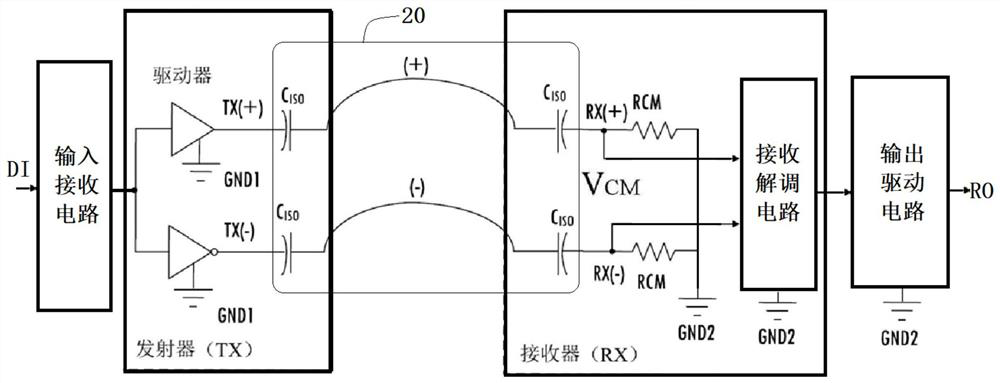
[0034] Input receiver circuit 1 first receives the figure 2 The transmission circuit shown in the figure couples in the positive terminal receiving signal RXP and the negative terminal receiving signal RXN of the differential signal through the isolation capacitor, and after filtering, the positive terminal input signal Vip and the negative terminal input signal Vin are obtained; the positive terminal input signal Vip and the negative terminal input signal The signal Vin then enters the common-mode...
PUM
 Abstract
Description
Claims
Application Information


