Full adder
A technology of full adder and signal, applied in the field of full adder, can solve the problem of high power consumption of full adder
- Summary
- Abstract
- Description
- Claims
- Application Information
AI Technical Summary
Problems solved by technology
Method used
Image

Examples
Embodiment Construction
[0038] The following will clearly and completely describe the technical solutions in the embodiments of the present invention with reference to the accompanying drawings in the embodiments of the present invention. Obviously, the described embodiments are only some, not all, embodiments of the present invention. Based on the embodiments of the present invention, all other embodiments obtained by persons of ordinary skill in the art without creative efforts fall within the protection scope of the present invention.
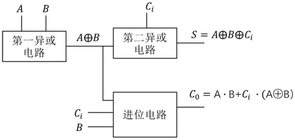
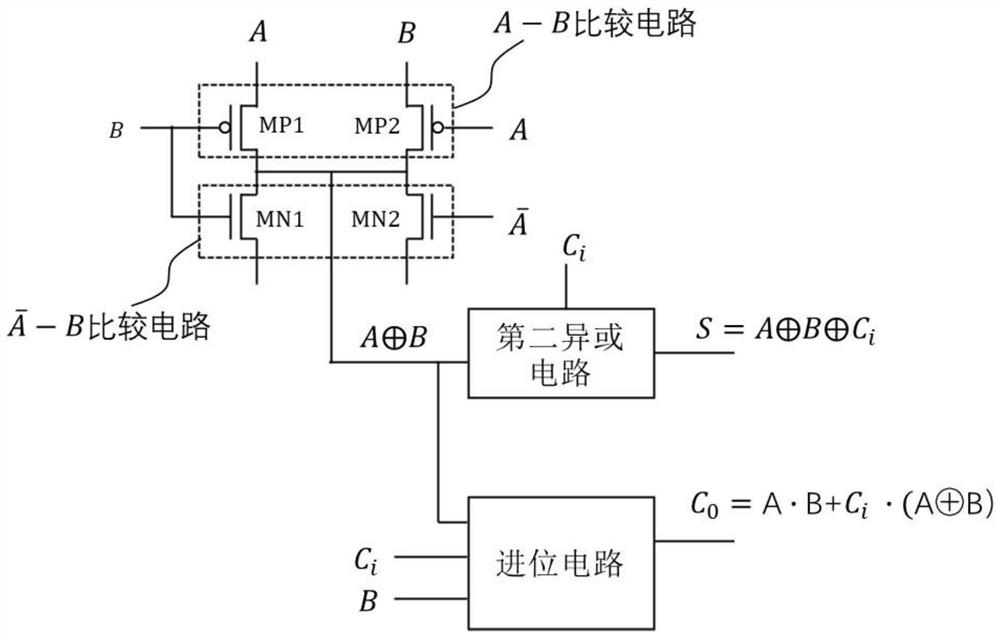
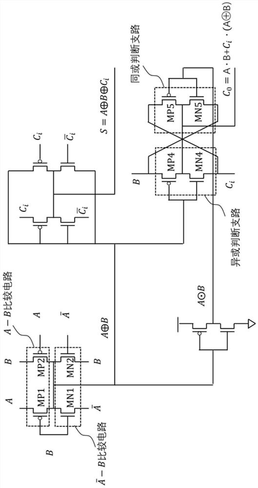
[0039] figure 1 A schematic circuit structure diagram of a full adder is provided for the embodiment of the present application.
[0040] Such as figure 1 As shown, the full adder in this embodiment includes: a first exclusive OR circuit, a second exclusive OR circuit, and a carry circuit.
[0041] The first exclusive OR circuit is used to access the first summation signal and the second summation signal, and the first exclusive OR circuit includes two sets of co...
PUM
 Abstract
Description
Claims
Application Information
 - R&D
- Intellectual Property
- Life Sciences
- Materials
- Tech Scout
- Unparalleled Data Quality
- Higher Quality Content
- 60% Fewer Hallucinations
Browse by: Latest US Patents, China's latest patents, Technical Efficacy Thesaurus, Application Domain, Technology Topic, Popular Technical Reports.
© 2025 PatSnap. All rights reserved.Legal|Privacy policy|Modern Slavery Act Transparency Statement|Sitemap|About US| Contact US: help@patsnap.com