Circuit board and manufacturing method thereof, and display screen

A manufacturing method and circuit board technology, which is applied in the field of display screens, can solve the problems of solder mask collapse or fall off, increased side erosion, and low reflectivity of circuit boards, so as to improve reflection, avoid side erosion, improve brightness and The effect of uniformity

Active Publication Date: 2022-08-09
QING DING PRECISION ELECTRONICS HUAIAN CO LTD +1
View PDF7 Cites 0 Cited by
  • Summary
  • Abstract
  • Description
  • Claims
  • Application Information

AI Technical Summary

Problems solved by technology

And the larger the aperture difference, it is easy to cause the solder mask adjacent to the window to collapse or fall off
And when the connection pad of the circuit board is connected to the light-emitting element, the reflectivity of the circuit board to light is relatively low
In order to meet the requirements of high reflectivity, the higher the content of titanium dioxide in the solder resist layer, but this component will reflect the ultraviolet light emitted by the exposure machine, so that the ink at the bottom of the solder resist layer cannot be cured and further increase the side etching

Method used


Image

  • Circuit board and manufacturing method thereof, and display screen
  • Circuit board and manufacturing method thereof, and display screen
  • Circuit board and manufacturing method thereof, and display screen

Examples


Embodiment Construction

[0054] The technical solutions in the embodiments of the present invention will be clearly and completely described below with reference to the accompanying drawings in the embodiments of the present invention. Obviously, the described embodiments are only a part of the embodiments of the present invention, rather than all the embodiments. Based on the embodiments of the present invention, all other embodiments obtained by those of ordinary skill in the art without creative efforts shall fall within the protection scope of the present invention.

[0055] Unless otherwise defined, all technical and scientific terms used herein have the same meaning as commonly understood by one of ordinary skill in the art to which this invention belongs. The terms used herein in the description of the present invention are for the purpose of describing specific embodiments only, and are not intended to limit the present invention.

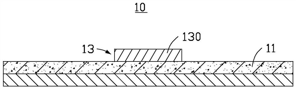
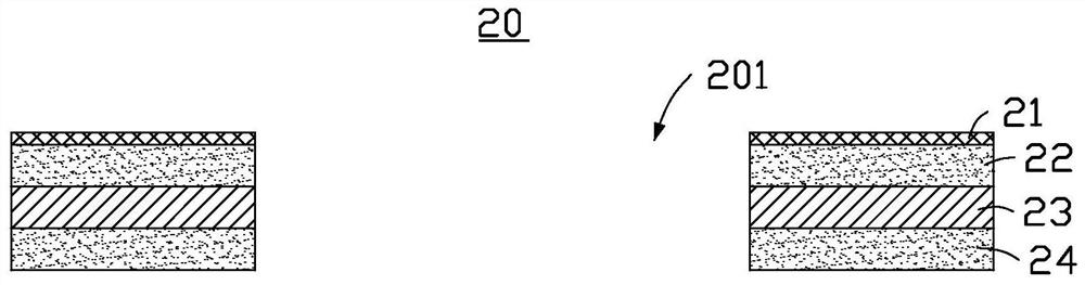
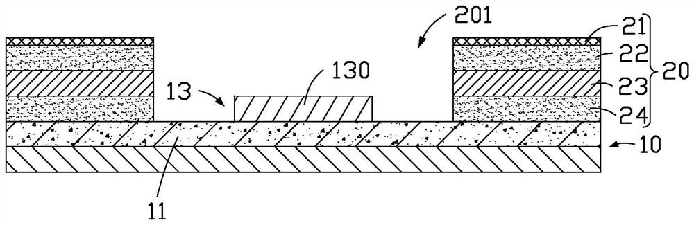
[0056] Some embodiments of the present invention will be desc...


PUM

PropertyMeasurementUnit
thicknessaaaaaaaaaa

Abstract

A circuit board includes a circuit substrate and a lamination film disposed on the circuit substrate, the circuit substrate includes a dielectric layer and a circuit layer formed on the dielectric layer, and the circuit layer includes at least one connection The lamination film includes a transparent adhesive layer, a metal layer and an adhesive layer that are stacked in sequence, the adhesive layer is combined with the dielectric layer on the side away from the metal layer, and the lamination film corresponds to each The connection pad is provided with an opening to expose the connection pad from the lamination film, and the aperture of each opening gradually increases from an end close to the dielectric layer to an end away from the circuit substrate. The circuit board is beneficial to avoid collapse of openings and improve reflectivity. The present invention also needs to provide a manufacturing method of a circuit board and a display screen using the circuit board.

Description

technical field [0001] The present invention relates to a circuit board and a manufacturing method thereof, and a display screen using the circuit board. Background technique [0002] With the development of miniaturization, light weight, high speed, multi-function and high reliability of electronic equipment, the semiconductor components in electronic equipment are also developing towards multi-pin and fine pitch, and it is required to carry electronic components ( Circuit boards such as LEDs are also developing towards miniaturization, light weight and high density. [0003] When the circuit board is connected to other electronic components, the connection pads need to be exposed from the solder resist layer. In order to ensure accuracy, windows are often opened on the solder resist layer by exposure. However, when the thickness of the solder resist layer is thicker, the difference between the upper and lower apertures of the opening formed by exposure is greater, that is...

Claims


Application Information

Patent Timeline
Patent Type & Authority Patents(China)
IPC IPC(8): H05K1/11H05K1/02H05K3/00H05K3/40
CPCH05K1/111H05K1/0274H05K3/0058H05K3/40
Inventor 吴金成黄美华侯宁
Owner QING DING PRECISION ELECTRONICS HUAIAN CO LTD
Why Eureka
Try Eureka