

Circuit board electronic element target detection method based on simplified YOLOv3 network.
An electronic component and target detection technology, applied in neural learning methods, computer parts, image data processing, etc., can solve the problem of low recognition accuracy of neural network models, reduce the number of segmentations, improve accuracy, and improve detection speed. Effect
- Summary
- Abstract
- Description
- Claims
- Application Information
AI Technical Summary
Problems solved by technology
Method used
Image

Examples
Embodiment Construction
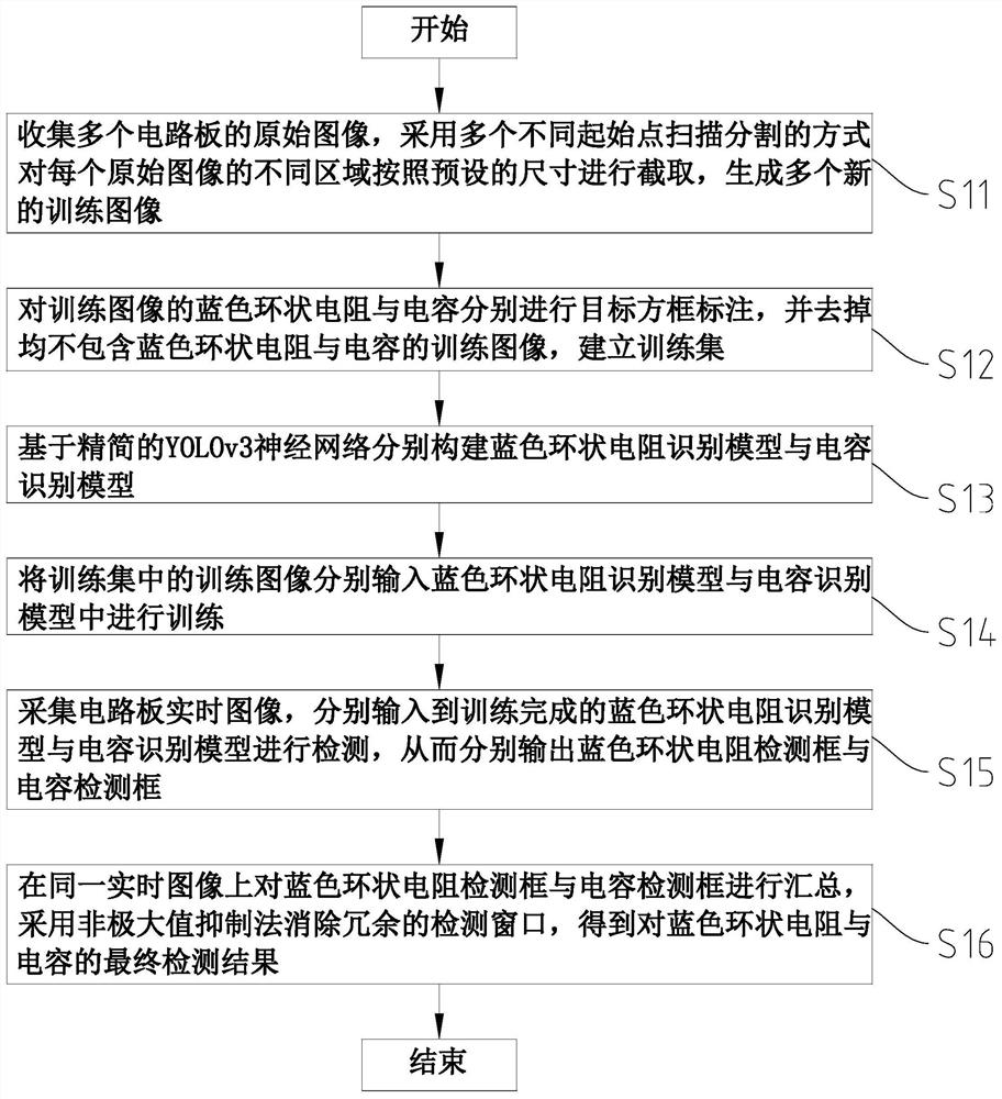
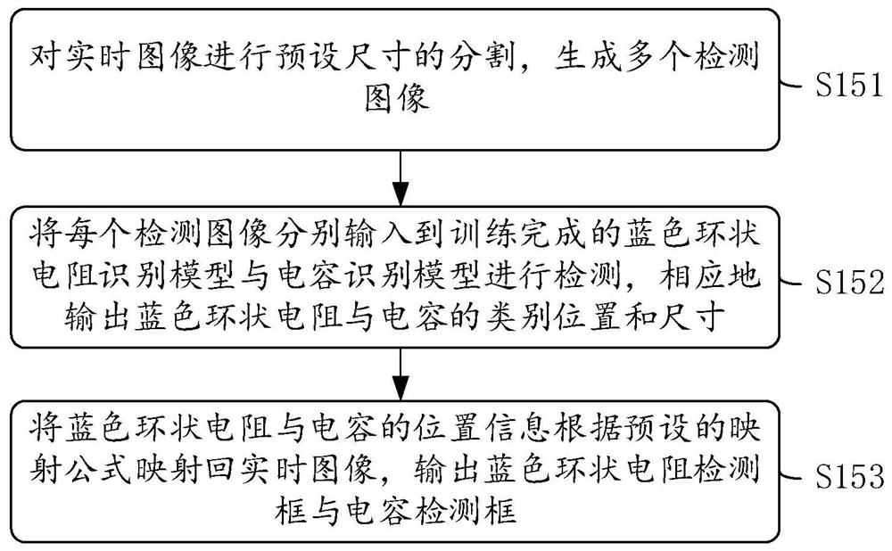
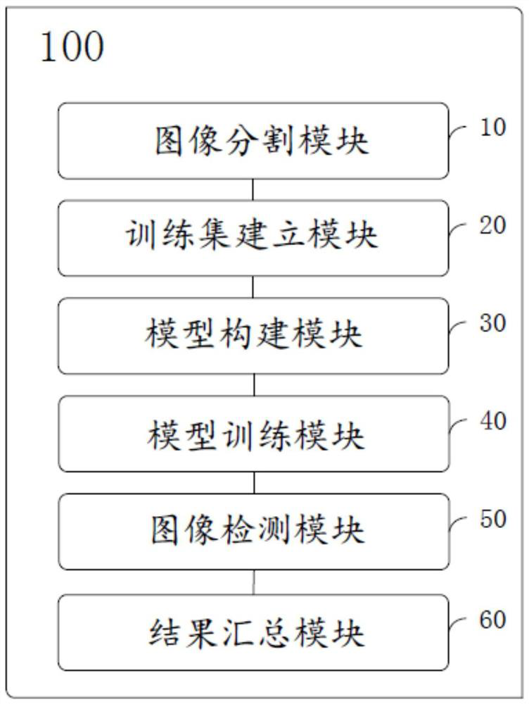
[0042] In order to make the object, technical solution and beneficial technical effects of the present invention clearer, the present invention will be further described in detail below in conjunction with the accompanying drawings and specific embodiments. It should be understood that the specific implementations described in this specification are only for explaining the present invention, not for limiting the present invention.
[0043] It should also be understood that the terminology used in the description of the present invention is for the purpose of describing particular embodiments only and is not intended to be limiting of the present invention. As used in this specification and the appended claims, the singular forms "a", "an" and "the" are intended to include plural referents unless the context clearly dictates otherwise.
[0044] It should also be further understood that the term "and / or" used in the description of the present invention and the appended claims re...
PUM
 Abstract
Description
Claims
Application Information