

Semiconductor thermoelectric material cutting device
A technology of thermoelectric material and cutting device, applied in metal processing and other directions, can solve the problem of cutting dust polluting the air, etc., and achieve the effect of reducing pollution
- Summary
- Abstract
- Description
- Claims
- Application Information
AI Technical Summary
Problems solved by technology
Method used
Image

Examples
Embodiment 1
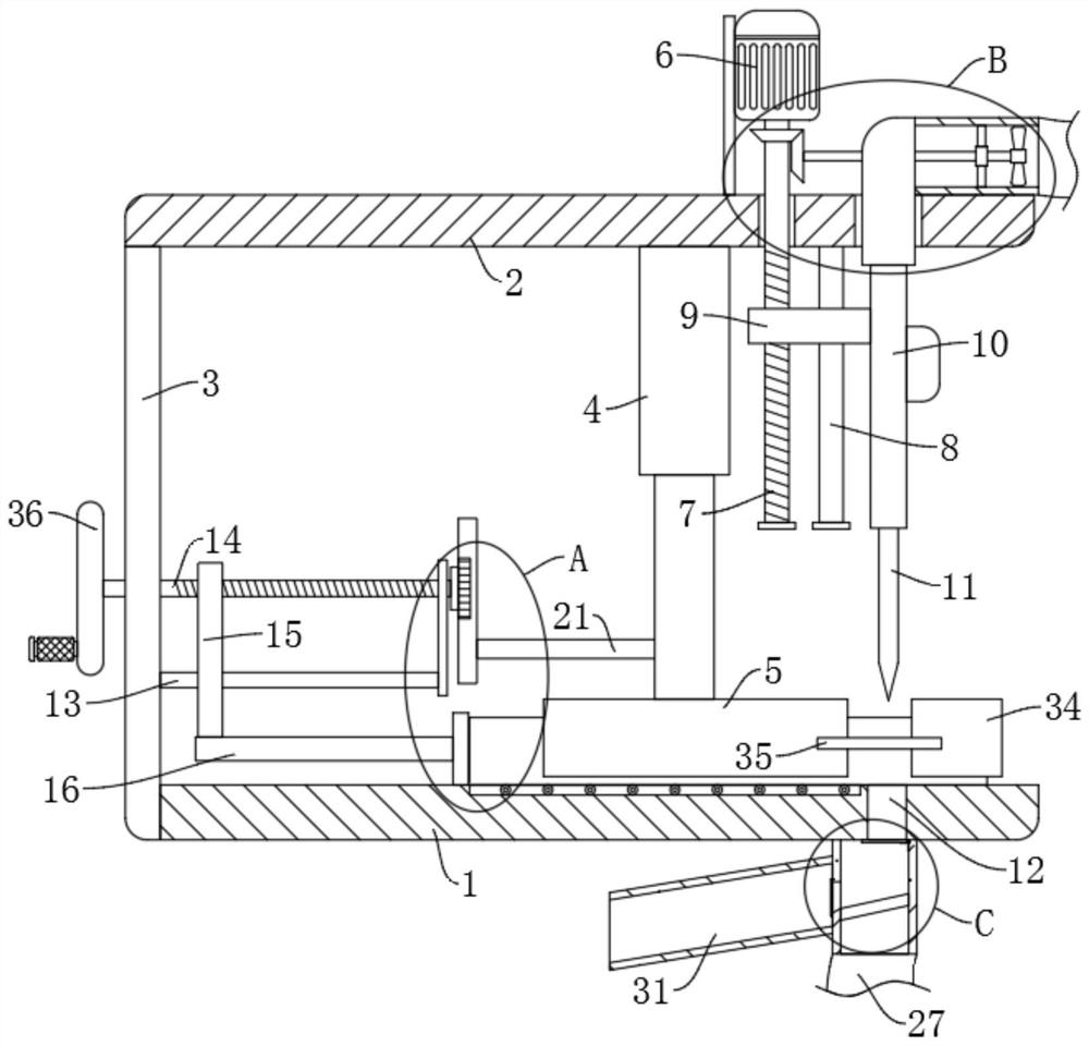
[0030] refer to Figure 1-5 , a semiconductor thermoelectric material cutting device, comprising a workbench 1, the upper end of the workbench 1 is fixedly connected with a top plate 2 through a vertical plate 3, the lower end of the top plate 2 is fixedly installed with a fixed plate 5 through a telescopic device 4, and the upper end of the top plate 2 is fixedly installed There is a driving motor 6, the output end of the driving motor 6 is fixedly connected with a first threaded rod 7 extending to the lower end of the top plate 2, and the lower end of the top plate 2 is fixedly connected with a first guide rod 8 arranged in parallel with the first threaded rod 7, the first The outer wall of the threaded rod 7 and the first guide rod 8 is provided with the first slide block 9 matched therewith, the side wall of the first slide block 9 is fixedly equipped with a casing 10, and a cutting device 11 is fixedly installed in the casing 10, and the working The upper end of the table...
Embodiment 2
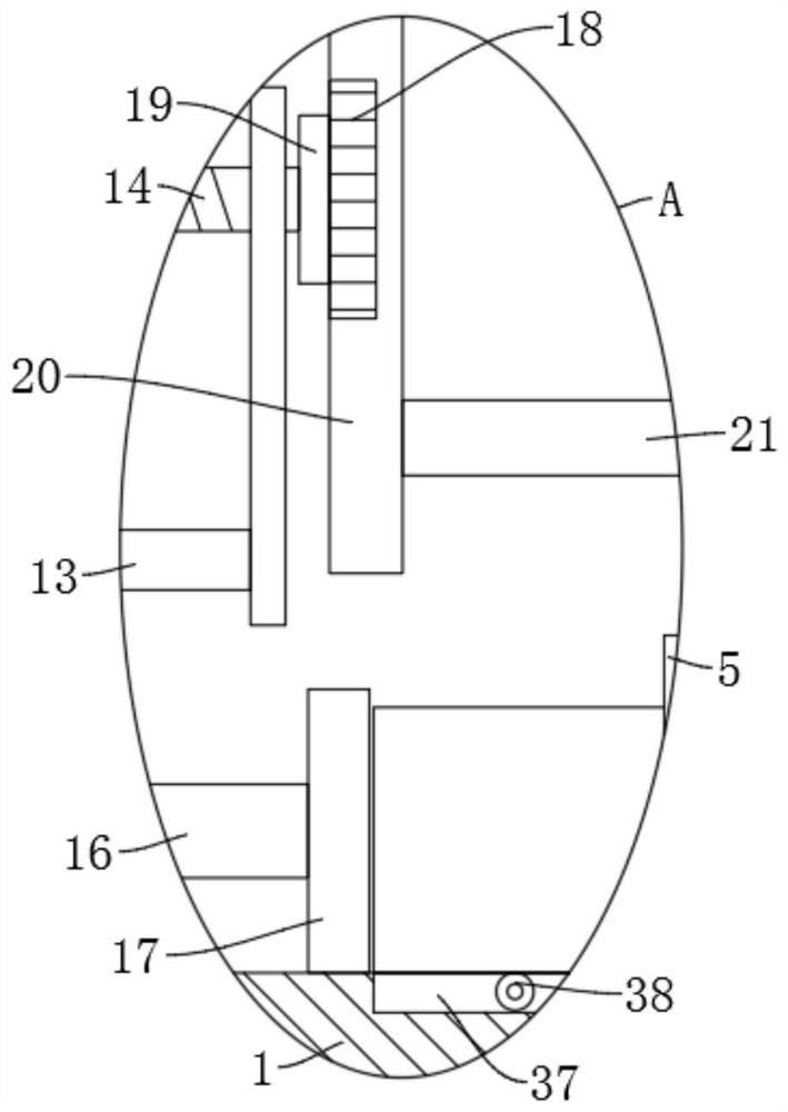
[0034] refer to Figure 1-2, is basically the same as Embodiment 1, furthermore: the feeding mechanism includes a second threaded rod 14 that is rotatably connected to the side wall of the vertical plate 3, and the side wall of the vertical plate 3 is fixedly connected with a second threaded rod 14 that is parallel to the second threaded rod 14. The second guide rod 13, the outer wall of the second threaded rod 14 and the second guide rod 13 is provided with a second slide block 15, the lower end side wall of the second slide block 15 is fixedly connected with a push plate 17 by a push rod 16, and the second The right end of the threaded rod 14 is connected with the first gear 18 through the ratchet 19, and the side wall of the telescopic end of the telescopic device 4 is fixedly connected with the rack 20 meshing with the first gear 18 through the connecting rod 21. During the lift, the telescopic device 4 will drive the rack 20 to slide upward through the connecting rod 21, ...
Embodiment 3
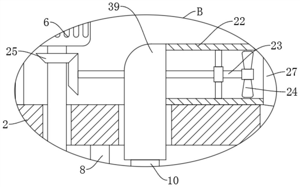
[0038] refer to figure 1 , image 3 and Figure 4 , is basically the same as Embodiment 1, furthermore: the dust suction mechanism includes a suction pipe 22 fixedly connected to the upper end of the top plate 2, and a rotating rod 23 is connected to the suction pipe 22 through a bracket to rotate, and the right end of the rotating rod 23 is fixedly installed Suction fan blade 24 is arranged, and the left end of rotating rod 23 and the output shaft of drive motor 6 are meshed and connected by two second gears 25. The lower end and the right end of the suction pipe 22 are fixedly connected and communicated through a flexible pipe 27. A filter plate 28 is fixedly installed in the ash suction pipe 26, and an ash discharge mechanism that cooperates with the filter plate 28 is provided in the ash suction pipe 26. When a threaded rod 7 rotates forward to drive the first slider 9 to slide downward, the first threaded rod 7 will drive the rotating rod 23 to rotate through the two se...
PUM
 Abstract
Description
Claims
Application Information