FPGA-based interface conversion method for different rates
An interface conversion and rate technology, applied in the field of FPGA communication, can solve the problems of insufficient storage resources and insufficient storage resources.
- Summary
- Abstract
- Description
- Claims
- Application Information
AI Technical Summary
Problems solved by technology
Method used
Image

Examples
Embodiment Construction
[0038] Embodiments of the present invention are described in detail below, examples of which are shown in the drawings, wherein the same or similar reference numerals designate the same or similar elements or elements having the same or similar functions throughout. The embodiments described below by referring to the figures are exemplary and are intended to explain the present invention and should not be construed as limiting the present invention.
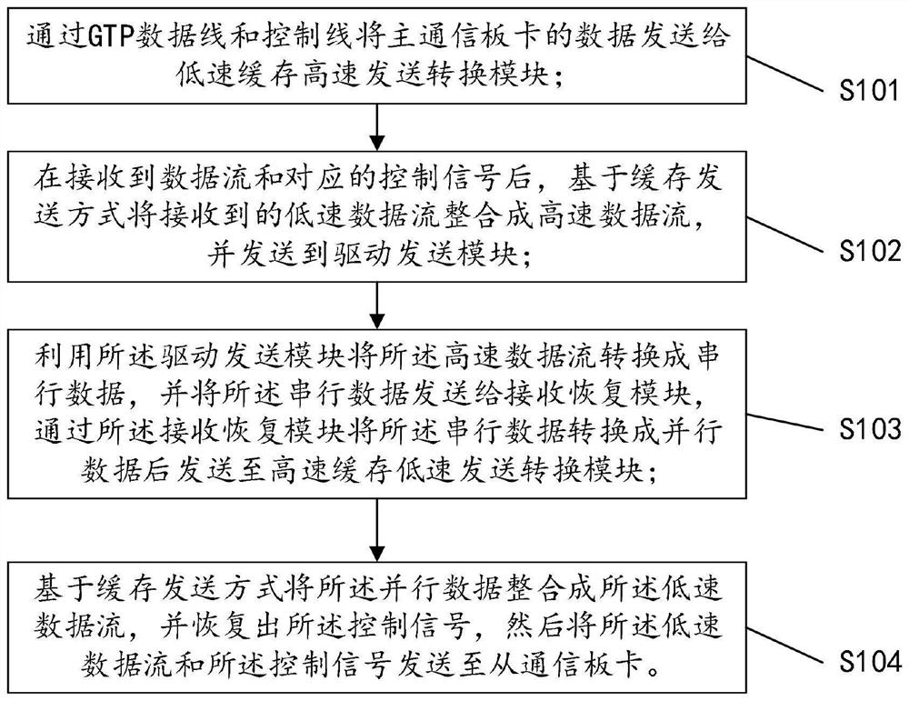
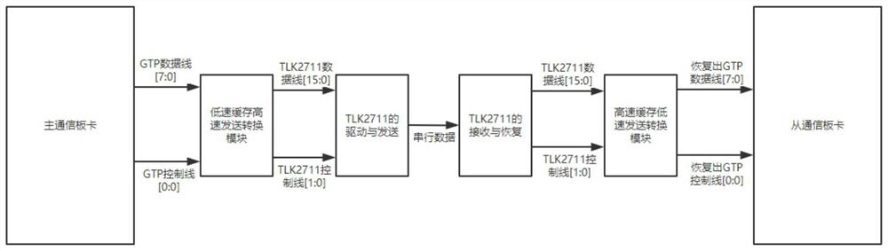
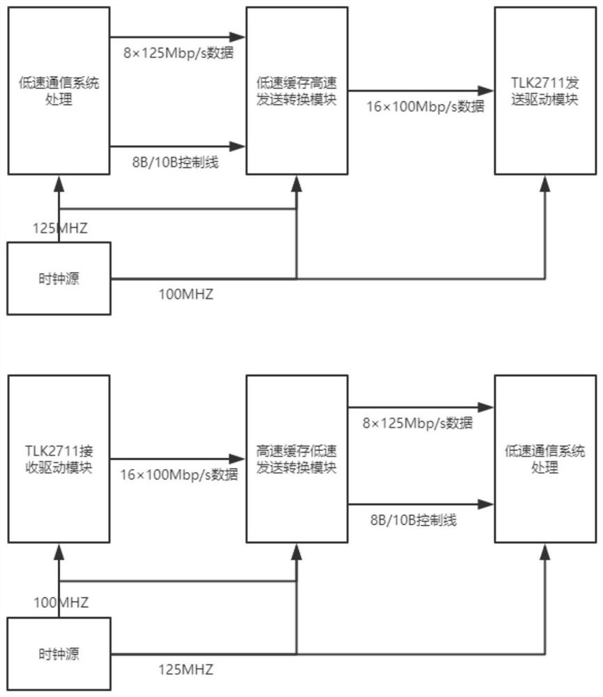
[0039] see Figure 1 to Figure 3 , the present invention provides a kind of interface conversion method based on the different rates of FPGA, comprises the following steps:
[0040] S101. Send the data stream of the main communication board to the low-speed cache and high-speed transmission conversion module through the data line and the control line of the GTP.
[0041] Specifically, the original communication system used XK7C325 chip of XILINX KINTEX-7 series. The GTP communication soft core that comes with the chip is used f...
PUM
 Abstract
Description
Claims
Application Information
 - R&D
- Intellectual Property
- Life Sciences
- Materials
- Tech Scout
- Unparalleled Data Quality
- Higher Quality Content
- 60% Fewer Hallucinations
Browse by: Latest US Patents, China's latest patents, Technical Efficacy Thesaurus, Application Domain, Technology Topic, Popular Technical Reports.
© 2025 PatSnap. All rights reserved.Legal|Privacy policy|Modern Slavery Act Transparency Statement|Sitemap|About US| Contact US: help@patsnap.com