A kind of heterojunction laser and preparation method thereof

A heterojunction and laser technology, applied in lasers, semiconductor lasers, phonon exciters, etc., can solve the problems of large temperature influence, poor directivity, monochromaticity and coherence, large beam divergence angle, etc. Lattice matching, particle number inversion, and simple process effects

Active Publication Date: 2022-08-02
SOUTHEAST UNIV
View PDF4 Cites 0 Cited by
  • Summary
  • Abstract
  • Description
  • Claims
  • Application Information

AI Technical Summary

Problems solved by technology

However, the laser performance of early semiconductor lasers is greatly affected by temperature, and the divergence angle of the beam is also large, so it is poor in directivity, monochromaticity and coherence.

Method used


Image

  • A kind of heterojunction laser and preparation method thereof
  • A kind of heterojunction laser and preparation method thereof

Examples


preparation example Construction

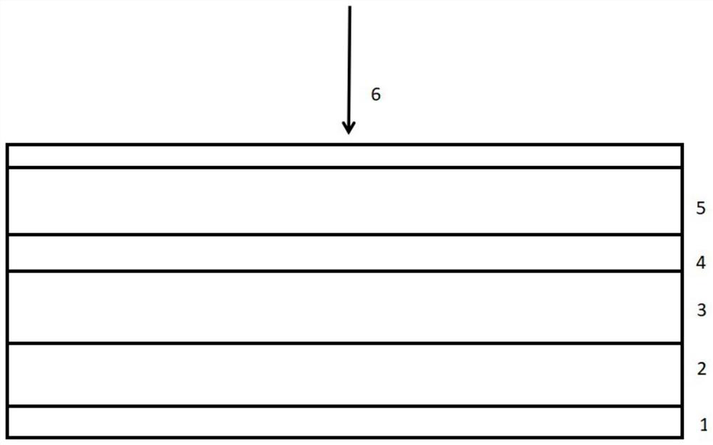
[0033] The preparation method of the heterojunction semiconductor laser of the present invention comprises the following steps:

[0034] a. Substrate preparation

[0035] In this patent, n-Si (111) sheet is used as the substrate, and the Si sheet is soaked in HF to remove the silicon dioxide on the surface, and then the Si sheet is cleaned several times with propanol, ethanol and deionized water to remove foreign matter on the surface of the silicon wafer. Dry the Si wafer with nitrogen and put it into a vacuum quartz tube for deposition treatment; heat the quartz tube to 300°C for 10-15min to remove the water vapor on the surface of the wafer;

[0036] b. GeS thin film preparation

[0037] 0.2g of germanium chloride dioxane complex, 0.4g of thiourea, and 20ml of oleamide OLA were added to a 25ml three-necked flask respectively, and were slightly magnetically stirred in the air; the stirred liquid mixture was ultrasonically treated for 5min, Remove the air in the oleylamine; t...

Embodiment

[0045] a. Substrate preparation

[0046] In this patent, n-Si (111) sheet is used as the substrate, and the Si sheet is soaked in HF to remove the silicon dioxide on the surface, and then the Si sheet is cleaned several times with propanol, ethanol and deionized water to remove the foreign matter on the surface of the silicon wafer. Dry the Si wafer with nitrogen and put it into a vacuum quartz tube for deposition treatment; heat the quartz tube to 300°C for 10-15min to remove the water vapor on the surface of the wafer;

[0047] b. GeS thin film preparation

[0048] 0.2g of germanium chloride dioxane complex, 0.4g of thiourea, and 20ml of oleamide OLA were added to a 25ml three-necked flask respectively, and were slightly magnetically stirred in the air; the stirred liquid mixture was ultrasonically treated for 5min, Remove the air in the oleylamine; then connect the three-necked flask to the Schlenk line, evacuate for 30 minutes to remove moisture and oxygen; pass nitrogen ...


PUM

PropertyMeasurementUnit
thicknessaaaaaaaaaa

Abstract

This invention discloses a heterojunction semiconductor laser and a preparation method thereof. The double-layer AD-type GeS stack and the double-layer rotating AB-type GeS stack can be laterally connected to form a type I semiconductor heterojunction, which is used in laser diodes. The particle number inversion can be realized in the medium, which can effectively reduce the working current. The semiconductor laser diode includes, from bottom to top, a lower electrode (1), a substrate (2), a lower cladding layer (3), an active layer (4), an upper cladding layer (5), and a contact layer (6). ) and the upper electrode (7). The material heterojunction selected in the present invention is easier to achieve lattice matching, and the preparation process is also simpler, and the double-layer rotating AD-type GeS stacking and the double-layer rotating AB-type GeS stacking can be carried out only by van der Waals force. Lateral connections form heterojunctions. In this paper, few-layer black phosphorene-like structures with different stacking structures are obtained by mechanical exfoliation.

Description

technical field [0001] The invention relates to a method for realizing a semiconductor laser with different stacking structures of few-layer SnS, and belongs to the technical field of semiconductor devices. Background technique [0002] Semiconductor laser is a general term for optical oscillators and optical amplifiers that use the electronic optical transitions in semiconductor materials to cause photon stimulated emission. Low-temperature pulsed lasing was observed in the earliest semiconductor lasers in 1962, and semiconductor lasers have developed rapidly since then. After years of efforts, due to the achievements of MBE and MOCVD technology, it has become possible to achieve precise control of the growth of semiconductor thin film materials, which has made significant progress in the development of semiconductor lasers, especially laser diodes, which are widely used in optical fiber communications, optical disks, Laser printers, laser scanners, laser pointers, etc., a...

Claims


Application Information

Patent Timeline
Patent Type & Authority Patents(China)
IPC IPC(8): H01S5/32
CPCH01S5/3222
Inventor 洪嘉祥雷双瑛江源长陈洁黄庆安
Owner SOUTHEAST UNIV
Why Eureka
Try Eureka