ZnO-based nanorod/ quantum well composite ultraviolet light-emitting diode and preparation method thereof

A technology of light-emitting diodes and nanorods, which is applied in the direction of electrical components, circuits, semiconductor devices, etc., can solve the problems of limiting the application of ZnO-based ultraviolet light emitters, poor interface quality, deep-level light emission, and low quantum efficiency of light-emitting diodes, and achieves weakening Polarization effects, improving the quality of materials and interfaces, and improving the effect of radiation recombination rate

Active Publication Date: 2017-04-26
SOUTH CENTRAL UNIVERSITY FOR NATIONALITIES
View PDF5 Cites 4 Cited by
  • Summary
  • Abstract
  • Description
  • Claims
  • Application Information

AI Technical Summary

Problems solved by technology

This scheme uses ZnO nanowires prepared by hydrothermal method as the light-emitting active layer, and its more defects and impurities will seriously affect the light-emitting efficiency.
[0005] In general, the existing ZnO-based ultraviolet light-emitting devices generally have the following problems: 1) The quantum confinement Stark effect caused by lattice mismatch and polarization effects leads to low quantum efficiency in light-emitting diodes; Poor interface quality and deep-level luminescence caused by material defects lead to poor UV monochromaticity of LEDs; 3) The light extraction efficiency caused by the traditional planar structure is low; 4) The preparation process is complicated, the conditions are strictly controlled, and high temperature preparation is required The high cost of preparation caused by factors such as
The aforementioned problems limit the application of ZnO-based UV emitters

Method used


Image

  • ZnO-based nanorod/ quantum well composite ultraviolet light-emitting diode and preparation method thereof
  • ZnO-based nanorod/ quantum well composite ultraviolet light-emitting diode and preparation method thereof
  • ZnO-based nanorod/ quantum well composite ultraviolet light-emitting diode and preparation method thereof

Examples


Embodiment 1

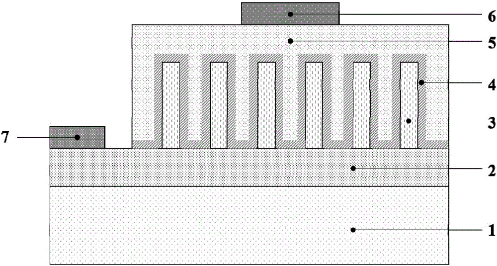
[0040] 1) Substrate cleaning: use sapphire as the substrate, cut it into a size of 15mm×15mm, ultrasonically clean it with acetone, alcohol and deionized water for 3 minutes, and finally use N 2 blow dry.

[0041] 2) Preparation of n-type ZnO thin film layer: Put the sapphire substrate after surface cleaning into the growth chamber of the radio frequency magnetron sputtering system, and the growth chamber is evacuated to the background pressure of 5×10 -4 Pa, heating the substrate to a temperature of 200°C. AZO ceramic target (ZnO:Al ceramic target) was selected as the target material for depositing n-type ZnO thin film layer. Before coating, pre-sputter for 10 min to remove impurities on the surface of the target, and then use radio frequency magnetron sputtering to deposit n-type ZnO thin film on the sapphire substrate. The temperature of the deposition substrate is 200° C., the gas during deposition is argon, the pressure is 0.5 Pa, the sputtering power is 60 W, and the s...

Embodiment 2

[0048] 1) Substrate cleaning: Use sapphire as the substrate, cut it into a size of 15mm×15mm, use acetone, alcohol, and deionized water to ultrasonically clean it for 3 minutes, and finally use N 2 blow dry.

[0049] 2) Preparation of n-type ZnO thin film layer: put the sapphire substrate after surface cleaning into the growth chamber of the radio frequency magnetron sputtering system, and vacuum the growth chamber to the background pressure of 1×10 -4 Pa, the substrate is heated to a temperature of 400 °C. AZO ceramic target is selected as the target material for depositing n-type ZnO thin film layer. Before coating, pre-sputter for 10 minutes to remove impurities on the surface of the target, and then use radio frequency magnetron sputtering to deposit an n-type ZnO thin film layer on the sapphire substrate; the temperature of the deposition substrate is 400 ° C, and the gas during deposition is Ar gas. The air pressure is 5.0Pa, the sputtering power is 150W, and the sputt...

Embodiment 3

[0056] 1) Substrate cleaning: Use sapphire as the substrate, cut it into a size of 15mm×15mm, use acetone, alcohol, and deionized water to ultrasonically clean it for 3 minutes, and finally use N 2 blow dry.

[0057] 2) Preparation of n-type ZnO thin film layer: put the sapphire substrate after surface cleaning into the growth chamber of the radio frequency magnetron sputtering system, and vacuum the growth chamber to the background pressure of 1×10 -3 Pa, heating the substrate to a temperature of 300°C. AZO ceramic target is selected as the target material for depositing n-type ZnO thin film layer. Before coating, pre-sputter for 10 min to remove impurities on the target surface. Then an n-type ZnO thin film layer was deposited on the sapphire substrate by radio frequency magnetron sputtering method. The temperature of the deposition substrate is 300° C., the gas during deposition is Ar gas, the gas pressure is 8.0 Pa, the sputtering power is 20 W, and the sputtering time ...


PUM


Abstract

The invention discloses a ZnO-based nanorod / quantum well composite ultraviolet light-emitting diode and a preparation method thereof. The light-emitting diode comprises a substrate. The substrate is provided with an n-type ZnO thin film layer, a ZnO nanorod array, a ZnO / Zn1-xMgxO quantum well active layer, a p-type NiO thin film layer and a first electrode from the bottom up in sequence. A second electrode and the ZnO nanorod array are arranged on the n-type ZnO thin film layer in parallel; and the ZnO / Zn1-xMgxO quantum well active layer covers the ZnO nanorod array, 0.1<=x<=0.3. The light-emitting diode electroluminescent peak wavelength is around 374 nm, and full width at half maximum of the photoluminescence peak is around 17 nm; the light-emitting diode structure can give full play to the advantages of direct broadband gap and high exciton binding energy of the ZnO material and the like, so that polarization effect is reduced effectively, material and interface quality can be improved, effective area of the active layer is increased, light extraction efficiency is improved and spectrum monochromaticity is improved; and besides, low-temperature preparation can be realized, cost is low and industrialization can be realized easily.

Description

technical field [0001] The invention relates to an optoelectronic device, in particular to a ZnO-based nanorod / quantum well composite ultraviolet light-emitting diode and a preparation method thereof. Background technique [0002] A light-emitting diode (LED) is a light-emitting element made of semiconductor material and a solid-state electroluminescence cold light source. Because light-emitting diodes have the characteristics of low energy consumption and environmental friendliness, their large-scale application will reduce the consumption of high-carbon energy such as coal and oil, which is in line with the requirements of sustainable development and the concept of low-carbon economy. Light-emitting diodes have been greatly favored for their advantages such as low power consumption, long life, high luminous efficiency, no radiation, and good portability, and related research and industries have received great support and development. In the field of LED research, the real...

Claims


Application Information

Patent Timeline
Patent Type & Authority Applications(China)
IPC IPC(8): H01L33/06H01L33/12H01L33/14H01L33/28H01L33/00
CPCH01L33/0087H01L33/06H01L33/12H01L33/14H01L33/28
Inventor 龙浩顾锦华钟志有王皓宁杨春勇侯金李颂战杨艳芹
Owner SOUTH CENTRAL UNIVERSITY FOR NATIONALITIES
Why Eureka
Try Eureka