A gallium nitride-based light-emitting diode and its preparation method

A light-emitting diode, gallium nitride-based technology, applied in electrical components, circuits, semiconductor devices, etc., can solve problems such as poor LED crystal quality, improve crystal quality, improve forward and side light output capabilities, and achieve diversification Effect

Active Publication Date: 2018-08-21
HC SEMITEK SUZHOU
View PDF2 Cites 0 Cited by
  • Summary
  • Abstract
  • Description
  • Claims
  • Application Information

AI Technical Summary

Problems solved by technology

[0006] In order to solve the problem of poor LED crystal quality in the prior art, an embodiment of the present invention provides a gallium nitride-based light-emitting diode and its preparation method

Method used


Image

  • A gallium nitride-based light-emitting diode and its preparation method
  • A gallium nitride-based light-emitting diode and its preparation method

Examples


Embodiment 1

[0031] An embodiment of the present invention provides a gallium nitride-based light emitting diode, see figure 1 , the gallium nitride-based light-emitting diode includes a sapphire substrate 1, and a buffer layer 2, an undoped GaN layer 3, a stress improvement layer 4, an N-type GaN layer 5, and an active layer 6 stacked sequentially on the sapphire substrate 1 , P-type electron blocking layer 7, and P-type GaN layer 8.

[0032] In this embodiment, the stress improvement layer 4 is composed of Al, Ga, and N in a volume ratio of 2:1 to 1:1. 2 and H 2 Formed under the atmosphere of the stress-improving layer 4, the surface is uneven. The sapphire substrate 1 adopts (0001) crystal orientation sapphire. The buffer layer 2 is a GaN layer or an AlGaN layer, and the active layer 6 includes alternately stacked InGaN layers and GaN layers. The P-type electron blocking layer 7 includes an AlGaN layer and an InGaN layer, or the P-type electron blocking layer 7 includes AlGaN.

[0...

Embodiment 2

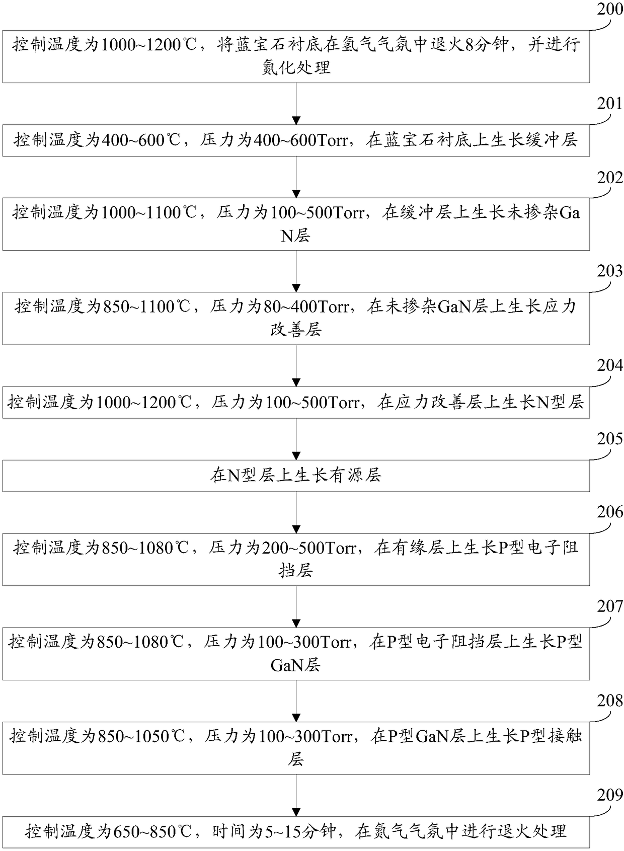
[0050]The embodiment of the present invention provides a method for preparing a gallium nitride-based light-emitting diode, which is suitable for preparing the gallium nitride-based light-emitting diode provided in Example 1, see figure 2 , the preparation method comprises:

[0051] Step 200: Control the temperature to 1000-1200° C., anneal the sapphire substrate in a hydrogen atmosphere for 8 minutes, and perform nitriding treatment.

[0052] Understandably, step 200 can clean the surface of the sapphire substrate.

[0053] In this embodiment, the sapphire substrate 1 adopts (0001) crystal orientation sapphire.

[0054] Step 201: Control the temperature to 400-600° C. and the pressure to 400-600 Torr to grow a buffer layer on the sapphire substrate.

[0055] In this embodiment, the buffer layer is a GaN layer.

[0056] Optionally, the thickness of the buffer layer may be 15-35 nm.

[0057] Optionally, after step 201, the preparation method may further include:

[0058] ...


PUM


Abstract

The invention discloses a gallium nitride based light emitting diode and a preparation method therefor, and belongs to the technical field of the semiconductor. The gallium nitride based light emitting diode comprises a sapphire substrate, and a buffer layer, a non-doped GaN (gallium nitride) layer, a stress improvement layer, an N type GaN layer, an active layer, a P type electron barrier layer and a P type GaN layer which are laminated on the sapphire substrate in sequence, wherein the stress improvement layer is formed by elements of Al, Ga and N under the atmosphere of N2 and H2 at a volume ratio of 2:1 to 1:1; and the surface of the stress improvement layer is uneven. According to the gallium nitride based light emitting diode, the stress improvement layer which is formed by the elements of Al, Ga and N under the atmosphere of N2 and H2 at a volume ratio of 2:1 to 1:1 is laminated between the non-doped GaN layer and the N type GaN layer, so that the lattice mismatch between the sapphire and the GaN is relieved, and the crystal quality of the light emitting diode is improved.

Description

technical field [0001] The invention relates to the technical field of semiconductors, in particular to a gallium nitride-based light-emitting diode and a preparation method thereof. Background technique [0002] Light Emitting Diode (LED for short) is a semiconductor electronic component that can emit light. Gallium nitride (GaN)-based materials have excellent properties such as wide direct bandgap, strong chemical bonds, high temperature resistance, and corrosion resistance. They are ideal materials for producing short-wavelength high-brightness light-emitting devices, ultraviolet light detectors, and high-temperature and high-frequency microelectronic devices. Widely used in full-color large-screen display, LCD backlight, signal lights, lighting and other fields. [0003] Existing GaN-based LEDs include a sapphire substrate, a buffer layer, an undoped GaN layer, an N-type GaN layer, an active layer, a P-type AlGaN layer, and a P-type GaN layer sequentially stacked on the...

Claims


Application Information

Patent Timeline
Patent Type & Authority Patents(China)
IPC IPC(8): H01L33/12H01L33/10H01L33/00H01L33/32
CPCH01L33/007H01L33/10H01L33/12H01L33/32
Inventor 王群郭炳磊董彬忠李鹏王江波
Owner HC SEMITEK SUZHOU
Why Eureka
Try Eureka