Semiconductor detection taping process and system

A semiconductor and braiding technology, which is applied in the direction of transportation packaging, packaging, packaging protection, etc., can solve the problems that the defective rate of the carrier tape is difficult to reduce, and it is impossible to accurately identify whether the positive and negative electrodes of the material are placed correctly, so as to reduce the defective rate.

Pending Publication Date: 2021-08-06
深圳市奥尼电通有限公司
View PDF10 Cites 0 Cited by
  • Summary
  • Abstract
  • Description
  • Claims
  • Application Information

AI Technical Summary

Problems solved by technology

[0002] The traditional braiding machine has the following disadvantages: it can only detect whether the material (i.e. semiconductor) can be powered on normally, and cannot accurately identify whether the positive and negative electrodes of the material are placed correctly, resulting in the possibility of reverse placement when the material is placed into the carrier tape , so that it is difficult to reduce the defect rate of the carrier tape

Method used


Image

  • Semiconductor detection taping process and system
  • Semiconductor detection taping process and system

Examples


Embodiment 1

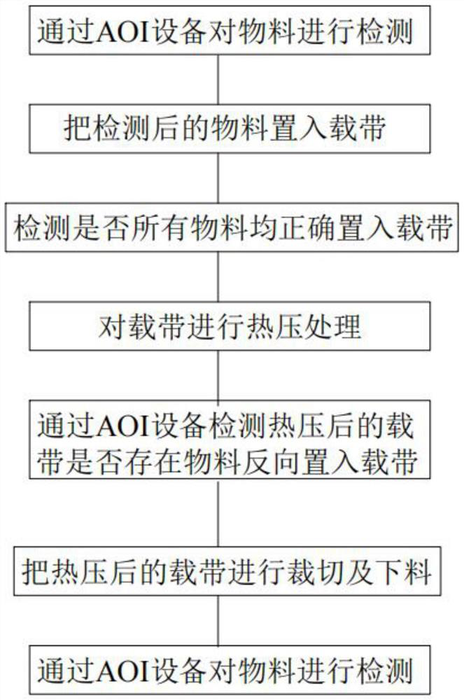
[0031] Such as figure 1 As shown, the present embodiment provides a semiconductor detection tape process, comprising the following steps:

[0032] A. Detect materials through AOI equipment;

[0033] B. Put the detected material into the carrier tape;

[0034] C. Carry out hot pressing treatment to the carrier tape;

[0035] D. Cut and unload the hot-pressed carrier tape.

[0036] Compared with the prior art that only detects whether the material can work normally, the present invention uses AOI equipment to detect the material, specifically to detect the appearance of the material, so as to identify whether the posture of the material is correct; in addition, the detection of the appearance of the material can also judge Whether there is wear and tear on the two power terminals of the material, so as to realize the detection of whether the material can be energized.

[0037] In summary, the use of AOI for detection also has the following advantages:

[0038] 1. The pixels...

Embodiment 2

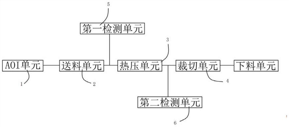
[0049] Such as figure 2 As shown, this embodiment provides a semiconductor detection tape system, including

[0050] AOI unit 1, used for visual inspection of materials;

[0051] The feeding unit 2 is used to put the detected material into the carrier tape;

[0052] The hot-pressing unit 3 is used for hot-pressing the carrier tape after placing the material;

[0053] The cutting unit 4 is used for cutting the hot-pressed carrier tape.

[0054] This embodiment can be used to implement the process described in Embodiment 1, that is, the AOI unit 1 is used to inspect the appearance of the material before braiding to detect whether its appearance is worn and whether its posture is accurate, and it can be judged according to the appearance that it can be reliably connected to electricity. And whether it is reversed, so that when the material is placed on the carrier tape, there will be no phenomenon of power failure or reversed connection, which improves the yield rate.

[005...


PUM


Abstract

The invention relates to the technical field of semiconductor assembly, in particular to a semiconductor detection taping process and a system capable of realizing the process. The process comprises the following steps of A, detecting a material through AOI equipment; B, placing the detected material into a bearing belt; C, carrying out hot pressing treatment on the bearing belt; and D, cutting and discharging the hot-pressed bearing belt. According to the semiconductor detection taping process and the system capable of realizing the process, the AOI equipment is used for detecting the material, the appearance of the material can be effectively detected, therefore whether the material is placed reversely or not is recognized, and the posture of the material can be conveniently adjusted in time so that the material can be prevented from being placed reversely in the bearing belt, and the reject ratio is reduced.

Description

technical field [0001] The invention relates to the technical field of semiconductor assembly, in particular to a semiconductor detection and braiding process and system. Background technique [0002] The traditional braiding machine has the following disadvantages: it can only detect whether the material (i.e. semiconductor) can be powered on normally, and cannot accurately identify whether the positive and negative electrodes of the material are placed correctly, resulting in the possibility of reverse placement when the material is placed into the carrier tape , so that it is difficult to reduce the defect rate of the carrier tape. Contents of the invention [0003] Aiming at the problems in the prior art, the present invention provides a semiconductor detection and braiding process and system, which can perform high-precision detection on materials, thereby ensuring that the materials will not be reversed in the carrier tape. [0004] In order to solve the above techn...

Claims


Application Information

Patent Timeline
Patent Type & Authority Applications(China)
IPC IPC(8): B65B57/10B65B15/04B65B51/10B65B61/06
CPCB65B57/10B65B15/04B65B51/10B65B61/06
Inventor 林逸宁何翠碧
Owner 深圳市奥尼电通有限公司
Why Eureka
Try Eureka