

CMP (chemical mechanical polishing) method
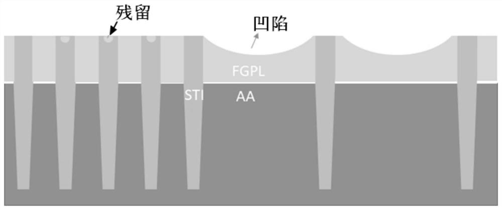
A grinding method and polysilicon thin film technology, which is applied in the field of CMP grinding, can solve problems such as dents and polysilicon residues, and achieve the effect of solving dents and residual problems
- Summary
- Abstract
- Description
- Claims
- Application Information
AI Technical Summary
Problems solved by technology
Method used
Image

Examples
Embodiment Construction
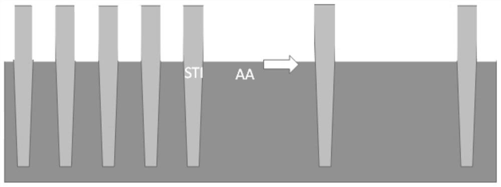
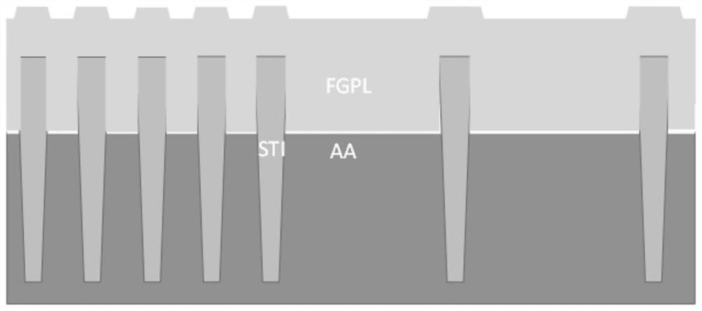
[0026] The specific embodiments of the present invention are given below in conjunction with the accompanying drawings, and the technical solutions in the present invention are clearly and completely described, but the present invention is not limited to the following embodiments. Apparently, the described embodiments are some, not all, embodiments of the present invention. Advantages and features of the present invention will be apparent from the following description and claims. It should be noted that all the drawings are in very simplified form and use imprecise ratios, which are only used for the purpose of conveniently and clearly assisting in describing the embodiments of the present invention. All other embodiments obtained by persons of ordinary skill in the art without creative efforts fall within the protection scope of the present invention.
[0027] This invention may be embodied in different forms and should not be construed as limited to the embodiments set for...
PUM
 Abstract
Description
Claims
Application Information