Formation method of semiconductor structure

A semiconductor and pattern layer technology, applied in the field of semiconductor structure formation, can solve the problems of poor pattern quality and affecting the yield of semiconductor structures, etc.

Active Publication Date: 2016-06-29
SEMICON MFG INT (SHANGHAI) CORP
View PDF3 Cites 16 Cited by
  • Summary
  • Abstract
  • Description
  • Claims
  • Application Information

AI Technical Summary

Problems solved by technology

[0005] However, in the prior art, when the layer to be etched is etched with a patterned mask layer, the quality of the pattern formed in the layer to be etched is poor, which affects the yield of the formed semiconductor structure

Method used


Image

  • Formation method of semiconductor structure
  • Formation method of semiconductor structure
  • Formation method of semiconductor structure

Examples


Embodiment Construction

[0036] It can be seen from the background art that the yield rate of semiconductor structures formed in the prior art needs to be improved.

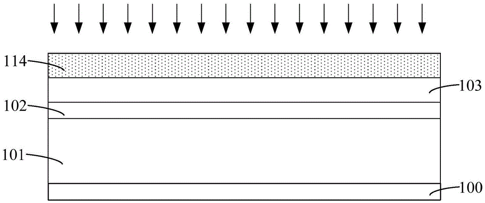
[0037] It has been found through research that oxide materials are usually used as a mask layer in the prior art, and a photoresist layer or a laminated structure of a bottom anti-reflection layer and a photoresist layer is formed on the surface of the mask layer, and there are openings in the photoresist layer; Then, using the photoresist layer with openings as a mask, the mask layer is etched, and the opening pattern of the photoresist layer is transferred into the mask layer.

[0038] When the opening feature size of the photoresist layer is small, if the thickness of the photoresist layer is too thick, the opening morphology of the photoresist layer will be deteriorated, and even easily lead to the collapse of the photoresist layer. Therefore, with the continuous reduction of the size of the semiconductor structure, the characteristi...


PUM


Abstract

A method for forming a semiconductor structure, comprising: providing a base; forming an initial mask layer on the base; performing doping treatment on the initial mask layer to convert the initial mask layer into a doped mask layer; A first pattern layer having a first opening is formed on the surface of the doping mask layer; using the first pattern layer as a mask, a dry etching process is used to etch the doping mask layer along the first opening, forming a second opening through the doping mask layer, and the etching rate of the doping mask layer in the dry etching process is higher than the etching rate of the initial mask layer; removing the first pattern layer. The etching rate of the doped mask layer in the dry etching process of the present invention is greater than the etching rate of the initial mask layer, so there is no need to form an organic distribution layer, avoiding the problem of residual organic distribution layer materials, and improving the initial mask layer and the second mask layer. Second, the cleanliness of the opening improves the yield rate of the formed semiconductor structure.

Description

technical field [0001] The invention relates to the technology in the field of semiconductor manufacturing, in particular to a method for forming a semiconductor structure. Background technique [0002] Semiconductor technology continues to move towards smaller process nodes driven by Moore's Law. With the continuous advancement of semiconductor technology, the functions of devices are becoming more and more powerful, but the difficulty of semiconductor manufacturing is also increasing day by day. Photolithography technology is the most critical production technology in the semiconductor manufacturing process. With the continuous reduction of semiconductor process nodes, the existing light source lithography technology can no longer meet the needs of semiconductor manufacturing. Extreme ultraviolet lithography (EUV), Multi-beam maskless technology and nanoimprint technology have become the research hotspots of next-generation lithography candidate technologies. However, th...

Claims


Application Information

Patent Timeline
Patent Type & Authority Applications(China)
IPC IPC(8): H01L21/033H01L21/3105
Inventor 张海洋张城龙
Owner SEMICON MFG INT (SHANGHAI) CORP
Why Eureka
Try Eureka