Chip double-sided photoelectric characteristic comprehensive detection system and device

A photoelectric characteristic and comprehensive detection technology, which is applied in the direction of measuring device, electronic circuit test, optical instrument test, etc., can solve the problems of high cost, different functions and structures of inspection tools, and single function of the detection system, so as to achieve simple design work, High application range and cost-saving effect

Pending Publication Date: 2021-08-10
英铂科学仪器(上海)有限公司
View PDF0 Cites 2 Cited by
  • Summary
  • Abstract
  • Description
  • Claims
  • Application Information

AI Technical Summary

Problems solved by technology

[0004] However, the current detection system has a single function
[0005] At present, the technical difficulty of the chip characteristic inspection tool is to customize it according to the needs of customers. The functions and structures of the inspection tools required by different customers are different. Every time the inspection tool is designed, it needs to be designed according to the customer's needs, which makes the design of the inspection tool complicated. , The cost is too high, the chip inspection tool designed each time can only be used for a specific chip, the application range of the inspection tool is low, and it cannot be adapted to the inspection and use of various chips

Method used


Image

  • Chip double-sided photoelectric characteristic comprehensive detection system and device
  • Chip double-sided photoelectric characteristic comprehensive detection system and device
  • Chip double-sided photoelectric characteristic comprehensive detection system and device

Examples


Embodiment 1

[0048] The air flotation base, sample adjustable fixture, front detection probe mechanism and back detection probe mechanism of this technology are modular mechanisms, which can be combined and assembled on the base, and the electrical characteristics of the chip can be tested and tested after assembly. detection. Its installation and use are flexible, and customers can choose to use and assemble it. It is not necessary to customize and design the corresponding detection mechanism every time different needs are required, the design work is simple and the cost is saved.

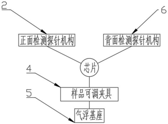
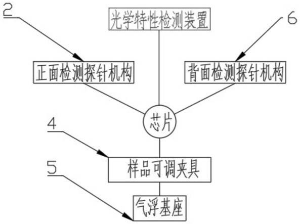
[0049] as attached figure 1 and 2 As shown, a chip double-sided photoelectric characteristic comprehensive detection system includes an air floating base 5, an adjustable sample fixture 4, a front detection probe mechanism 2 and a back detection probe mechanism 6, wherein:

[0050] The air-floating base 5 is used to use aerodynamic force as a mobile support to provide an air-floating force for the sample ad...

Embodiment 2

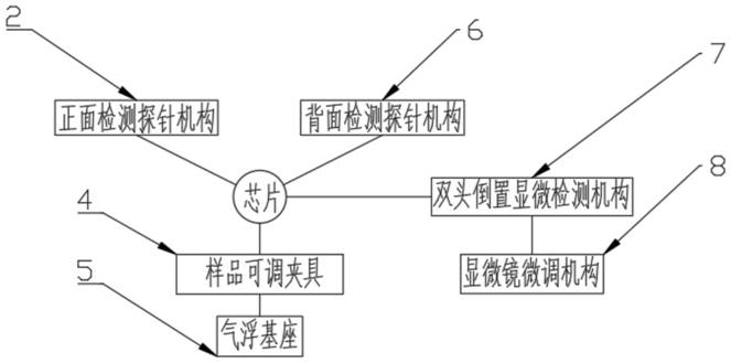
[0086] Based on the implementation of embodiment 1, in this embodiment, in order to facilitate the front detection probe mechanism 2 and the back detection probe mechanism 6 to carry out needle stick detection on the chip and microscopic observation of the structure of the chip, as attached figure 2 as shown,

[0087] A double-headed inverted microscopic detection mechanism 7 is also provided.

[0088] Preferably, it also includes a double-headed inverted microscopic detection mechanism 7, which is used to adjust the inverted double-headed microscope and drive the inverted double-headed microscope to perform surface microscopic observation and Needle stick test.

[0089]The double-headed inverted microscopic detection mechanism 7 includes an integrated double-sided microscope, which is in an inverted state, and is used to observe the front and back of the sample and realize needle pricking at the same time.

[0090] By moving the microscope base directly above the sample an...

Embodiment 3

[0096] A chip double-sided electronic characteristic detection device, including a kind of chip double-sided photoelectric characteristic comprehensive detection system described in the above embodiment 1 and / or embodiment 2; also includes a board base 1 and a gantry support 3, the gantry support 3 is vertically installed on the upper surface of the board base 1; the air float base 5 is fixed on the upper surface of the board base 1, and the front detection probe mechanism 2 and the back detection probe mechanism 6 are symmetrically fixed on the front side of the gantry support 3; The mechanism 8 is fixed on the board base 1 .

[0097] In order to install the chip double-sided photoelectric characteristic comprehensive detection system, hardware components are required to support and install the chip double-sided photoelectric characteristic comprehensive detection system.

[0098] as attached figure 2 and 4 As shown, the device also includes a board base 1 and a gantry bra...


PUM


Abstract

The invention discloses a chip double-sided photoelectric characteristic comprehensive detection system and device. The comprises an air floating base, a sample adjustable clamp, a front electrical detection probe mechanism, a back electrical detection probe mechanism, a front observation mechanism, a back observation mechanism and the like, the air floating base, the sample adjustable clamp, the front detection probe mechanism and the back detection probe mechanism are modularized mechanisms, and the sample adjustable clamp, the front detection probe mechanism and the back detection probe mechanism can be assembled on the base in a combined mode; and chip electrical characteristic testing and detection can be carried out after assembling is completed; and an optical characteristic detection device can be additionally arranged for optical characteristic detection, and functions are comprehensive. The system can be flexibly installed and used, and can be selectively used and assembled by a client. A corresponding detection mechanism does not need to be additionally customized and designed according to different needs every time, so that the design work is simple, and the cost is saved. According to the system, each mechanism can be selected and combined for use, so that the detection tool is wide in application range and can be adapted to detection of various chips.

Description

technical field [0001] The present application relates to the technical field of semiconductor chips, and in particular, to a comprehensive detection system and device for photoelectric characteristics on both sides of a chip. Background technique [0002] After the semiconductor chip is prepared, it is necessary to carry out data inspection and verification of its electrical characteristics, and it is necessary to use a probe to perform a needle test on the chip. Therefore, the chip characteristic inspection tool is used to detect the electrical characteristics of the chip sample, and is a necessary tool for designing, manufacturing and inspecting chips. [0003] In addition, if the semiconductor chip is an optoelectronic chip, data detection and verification of its optical characteristics is also required. The optoelectronic chip has active optical components, therefore, it is necessary to perform optical detection on the active optical components to ensure the applicabil...

Claims


Application Information

Patent Timeline
IPC IPC(8): G01D21/02G01R31/28G01M11/02
CPCG01D21/02G01M11/02G01M11/0207G01R31/2886
Inventor 陆冰彬
Owner 英铂科学仪器(上海)有限公司
Why Eureka
Try Eureka