PCB detection jig processing device and using method thereof

A technology of PCB board and detection jig, applied in the direction of measuring device, measuring device casing, measuring electrical variables, etc., can solve the problems of low detection efficiency and troublesome use, and achieve the effect of convenient and normal use and avoid normal detection effect.

Active Publication Date: 2021-08-13
深圳市顺天祥电子有限公司
View PDF8 Cites 2 Cited by
  • Summary
  • Abstract
  • Description
  • Claims
  • Application Information

AI Technical Summary

Problems solved by technology

[0006] The purpose of the present invention is: in order to solve the problem that existing detection equipment generally utilizes detection instruments, in order to facilitate the detection of connection points at different positions, it is necessary for workers to hold the detection head in contact with the PCB board, but such detection requires the staff to hold it for a long time The operation of the detection head is cumbersome to use and the detection efficiency is relatively low. At the same time, some bent PCB boards caused by accidents will be sprayed during the detection process. It is necessary to detect the PCB from an oblique angle, which further improves people's manual operation. Difficulty, which has caused some troubles for people to use, and the surface of the PCB board may be covered with a lot of dust before testing, and people need to use tools to remove dust to avoid more dust covering the connection points and affecting the detection effect of the PCB board problem, and proposed a PCB board detection fixture processing device and its use method

Method used


Image

  • PCB detection jig processing device and using method thereof
  • PCB detection jig processing device and using method thereof
  • PCB detection jig processing device and using method thereof

Examples


Embodiment 1

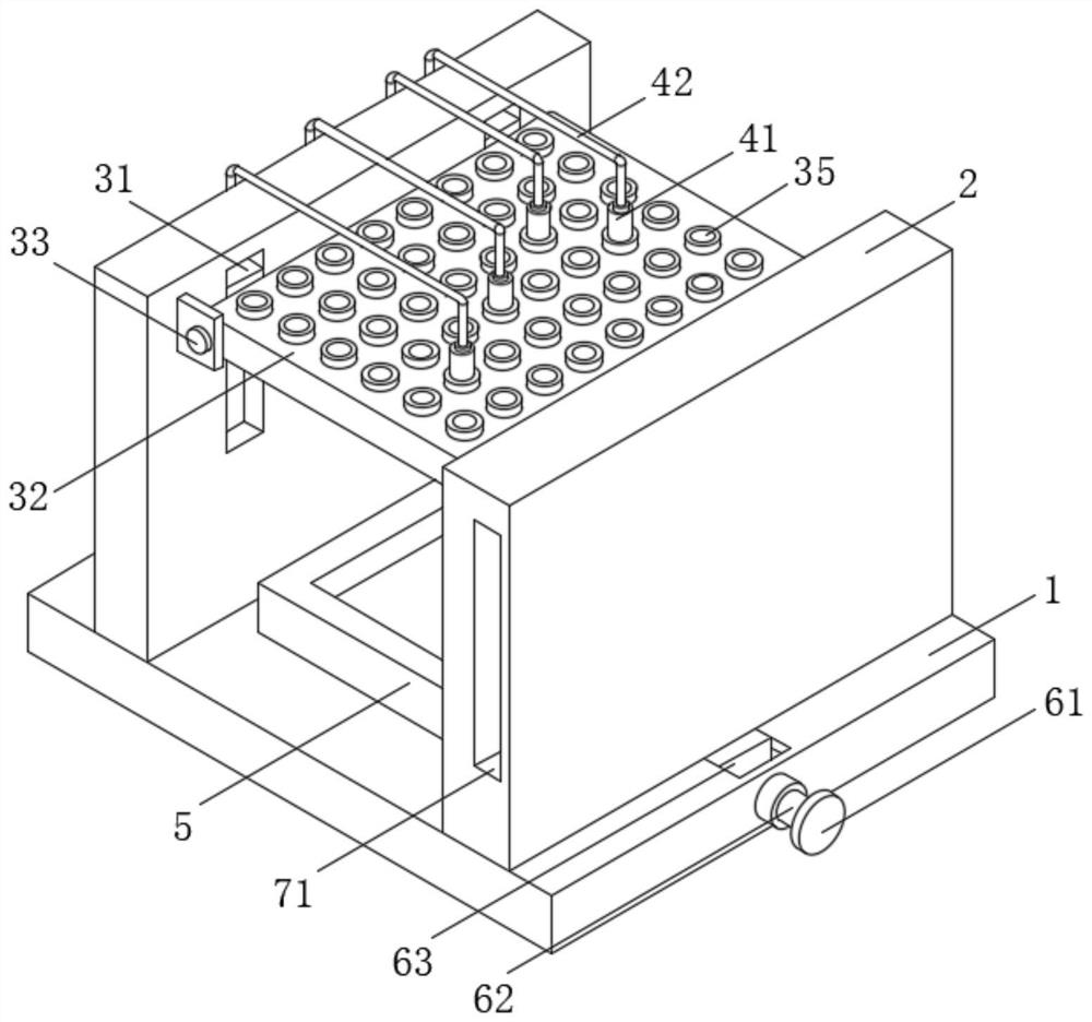
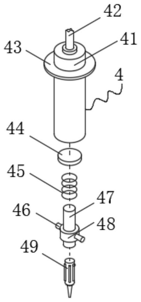
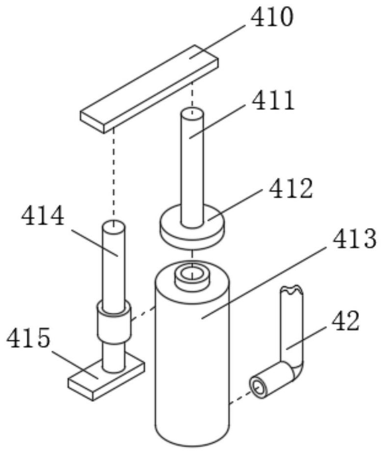
[0047] see Figure 1-7 , this embodiment discloses a PCB inspection fixture processing device, comprising a base plate 1 and a side plate 2, the left and right sides of the upper surface of the base plate 1 are provided with side plates 2, and the left side plate 2 is fixedly connected to the base plate 1, the lower surface of the right side plate 2 is attached to the upper surface of the bottom plate 1, and the lower surface of the right side plate 2 is fixedly connected with an adjustment mechanism 6 for adjusting the position of the side plate 2 and indirectly controlling the adjustment of the positioning mechanism 3. The adjustment mechanism 6 is arranged inside the base plate 1, and the adjustment mechanism 6 includes a second chute opened on the upper surface of the base plate 1, and a second slide block 63 is arranged in the second chute, and the upper surface of the second slide block 63 and the side The lower surface of the plate 2 is fixedly connected, the right side...

Embodiment 2

[0056] This embodiment discloses a method for using a PCB board detection fixture processing device, which specifically includes the following steps:

[0057] S1. Place the PCB board to be detected on the loading seat 5, and turn the screw block 61 to drive the threaded column 64 to rotate through the first rotating shaft 62. Under the action of the threaded cap, the second slider 63 can be stabilized along the track Left and right movement, the second slider 63 drives the side plate 2 to move and adjust the position, and the side plate 2 can be effectively kept fixed when it moves to any position;

[0058] S2. When the right side plate 2 moves close to the left side plate 2, the two side plates 2 approach each other and press against the positioning plate 32, and under the action of the fourth rotating shaft 36 and the fourth bearing, the positioning plate 32 is squeezed It can present an arc curved state. At this time, different rubber sleeves 35 on multiple positioning plat...


PUM


Abstract

The invention discloses a PCB detection jig machining device and a using method thereof, and belongs to the technical field of PCBs, the PCB detection jig machining device comprises a bottom plate and side plates, the side plates are arranged on the left side and the right side of the upper surface of the bottom plate, the left side plate is fixedly connected to the upper surface of the bottom plate, the lower surface of the right side plate is attached to the upper surface of the bottom plate, the lower surface of the right side plate is fixedly connected with an adjusting mechanism used for adjusting the position of the side plate and indirectly controlling the positioning mechanism to adjust, and the adjusting mechanism is arranged in the bottom plate. According to the invention, the detection mechanism is arranged, pressing blocks are controlled to drive a second sliding rod to move downwards, the second sliding rod drives a pressing rod to move downwards through a pressing plate, the pressing rod drives a piston block to move downwards, the piston block extrudes air in a second air cylinder, and a detection head can detect a connection point; in the detection process, multiple different pressing blocks are pressed, and a plurality of different detection heads move downwards and are matched with one another to achieve a good detection effect on different PCBs, so that normal use of people is greatly facilitated.

Description

technical field [0001] The invention belongs to the technical field of PCB boards, and in particular relates to a PCB board detection jig processing device and a use method thereof. Background technique [0002] PCB board, that is, printed circuit board, is the carrier for the installation of electronic components, and it is also the provider of electrical connections for electronic components. It is used for the connection of various tiny electronic components in the equipment. work normally. [0003] In order to ensure its normal operation, the PCB board needs to be tested with testing fixtures. Existing testing equipment generally uses testing instruments. In order to facilitate the detection of connection points at different positions, workers need to hold the detection head in contact with the PCB board. For example, Chinese invention patent CN201210459557.2 discloses a PCB test fixture, including a box body 1 , a pin plate 2 , a carrier plate 3 , a cover plate 4 and a...

Claims


Application Information

Patent Timeline
Patent Type & Authority Applications(China)
IPC IPC(8): G01R31/28G01R1/04
CPCG01R31/2808G01R1/0425Y02W30/82
Inventor 黄财仙刘本好
Owner 深圳市顺天祥电子有限公司
Why Eureka
Try Eureka