Photoetching mask for photoetching alignment of small-size patterns, and chip photoetching method

A technology of lithography alignment and lithography plate, which is applied in the field of photoelectric detection, can solve the problems that it is difficult for human eyes to recognize small-sized graphics, and it is impossible to prepare chips with small-sized graphics, and achieve the effect of saving available space

Active Publication Date: 2021-08-20
11TH RES INST OF CHINA ELECTRONICS TECH GROUP CORP
View PDF8 Cites 0 Cited by
  • Summary
  • Abstract
  • Description
  • Claims
  • Application Information

AI Technical Summary

Problems solved by technology

[0003] Embodiments of the present invention provide a photolithography plate and chip photolithography method for alignment of small-sized pattern photolithography, which is used to solve the problem of manual contact photolithography in the prior art, and it is difficult for human eyes to recognize small-sized patterns during the alignment process. , resulting in the inability to manufacture chips with small-sized graphics

Method used


Image

  • Photoetching mask for photoetching alignment of small-size patterns, and chip photoetching method
  • Photoetching mask for photoetching alignment of small-size patterns, and chip photoetching method
  • Photoetching mask for photoetching alignment of small-size patterns, and chip photoetching method

Examples


Embodiment 1

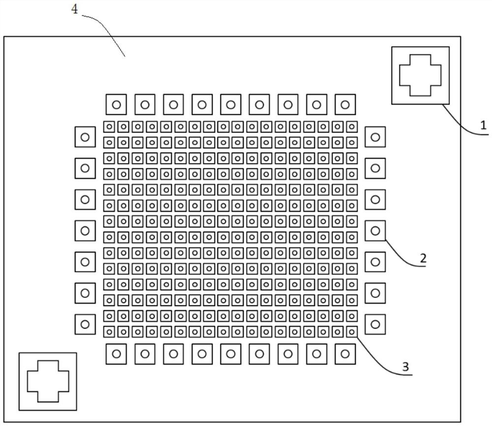
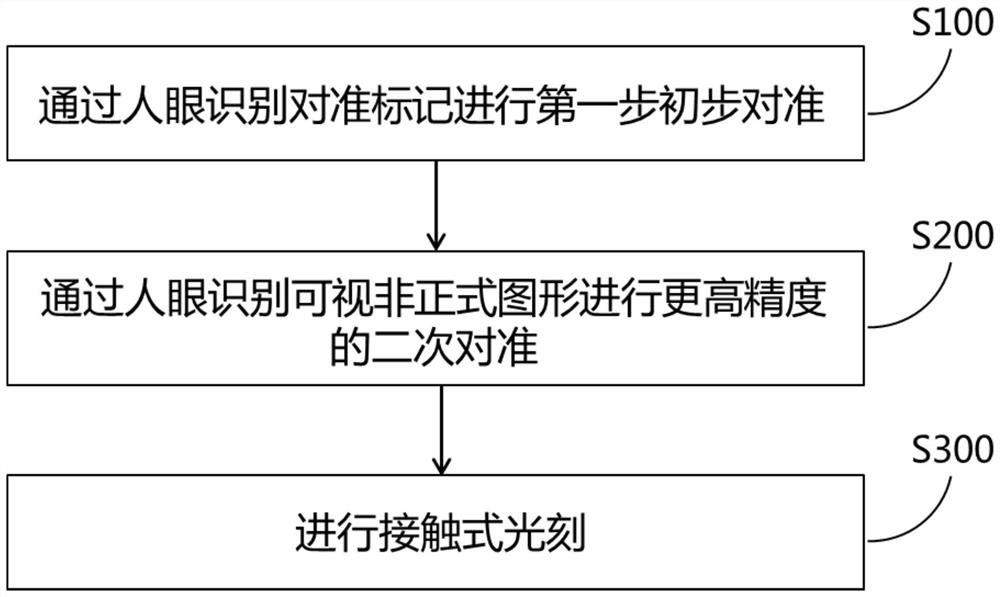
[0052] The photoresist plate used for photolithographic alignment of small-scale patterns in the embodiment of the present invention is suitable for photolithography of a chip. like figure 1 As shown, the photolithography plate includes three main parts: alignment marks 1, visible informal graphics 2, and invisible formal graphics 3. The size of the alignment mark 1 is designed to be very obvious and clearly visible according to the size of the chip and the actual available space, the shape is any complementary figure, the number is 2-4, and it is located at the four corners of the body 4 for preliminary alignment of photolithography; The size of the visible informal figure 2 is the smallest size that can be clearly recognized by the human eye under the field of view of the contact lithography machine used, and the shape is the invisible formal figure 3. Array form, and there is a corresponding law with the arrangement of the formal pattern, which is used for the final high-p...

Embodiment 2

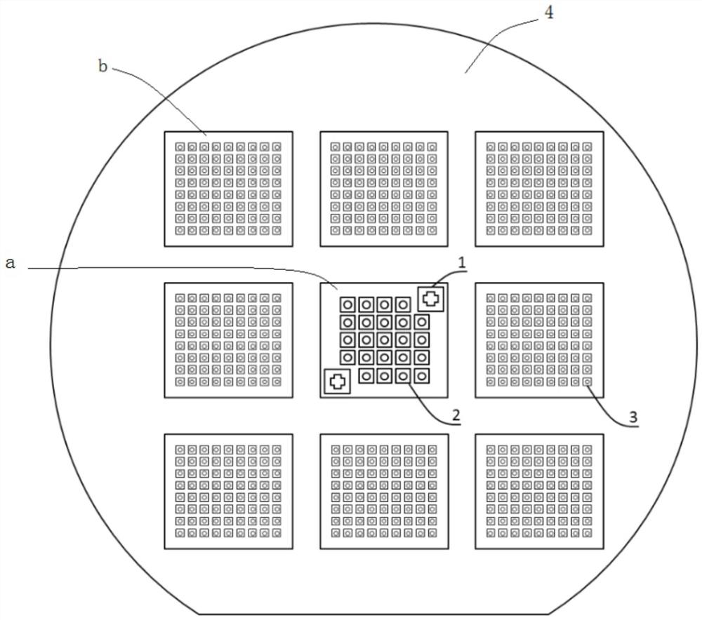
[0059] The photoresist plate used for photolithographic alignment of small-scale patterns in the embodiment of the present invention is suitable for photolithography of multiple chips at the same time. like figure 2 As shown, the photolithographic plate includes two main parts: the first area a and the second area b, wherein the size of the first area a is the same as that of the second area b, and the number and position can be determined according to the number of the second area b Reasonable adjustments are made; the size of the invisible official pattern 3 in the second region b is within the exposure accuracy range of the contact lithography machine used, but cannot be recognized by human eyes.

[0060] The first area a comprises two main parts: alignment marks 1 and visible informal graphics 2 . The size of the alignment mark 1 is designed to be very obvious and clearly visible according to the size of the chip and the actual available space. The shape is any complemen...


PUM


Abstract

The invention discloses a photoetching mask for photoetching alignment of small-size patterns, and a chip photoetching method. The photoetching mask for photoetching alignment of the small-size patterns comprises a body, at least one alignment mark, a plurality of visible informal patterns and a plurality of invisible formal patterns, the alignment mark, the plurality of visible informal patterns and the plurality of invisible formal patterns are arranged on the body, the alignment mark is larger than the visible informal patterns, and the visible informal patterns are larger than the invisible formal patterns; the alignment mark corresponds to a mark on the chip, and the visual informal graph corresponds to a graph on the chip; and a corresponding rule exists between the arrangement of the plurality of visible informal graphs and the arrangement of the plurality of invisible formal graphs. The preparation of small-size patterns which cannot be recognized and aligned by human eyes in a manual contact type photoetching process can be completed; and under the condition of one plate and multiple chips, not only is the alignment of graphs with smaller sizes realized, but also the available space of the formal chip is saved through an external alignment mode.

Description

technical field [0001] The invention relates to the field of photoelectric detection, in particular to a photolithography plate and a chip photolithography method for photolithography alignment of small-scale patterns. Background technique [0002] With the increasing demand for the performance and size of semiconductor chips in various fields, the preparation of semiconductor chips is developing in the direction of larger array size and smaller array size. In the manufacturing process of semiconductor chips, manual contact lithography is widely used in the fields of frontier research of science and technology and production of special process chips. The alignment process of manual contact lithography is usually divided into two steps. The first step is to use human eyes to identify the alignment marks on the photolithography plate and the chip, and perform manual adjustment to complete the initial first alignment. It uses human eyes to recognize the photolithography plate ...

Claims


Application Information

Patent Timeline
Patent Type & Authority Applications(China)
IPC IPC(8): G03F9/00
CPCG03F9/7046G03F9/7073Y02P70/50
Inventor 冯晓宇王成刚谢珩
Owner 11TH RES INST OF CHINA ELECTRONICS TECH GROUP CORP
Why Eureka
Try Eureka