Voltage self-following anti-backflow circuit

An anti-backfill and voltage technology, applied in the direction of adjusting electrical variables, instruments, control/regulation systems, etc., can solve the problem that the circuit cannot work, cannot achieve constant current charging anti-backfill and no voltage loss functions, and does not allow continuous changes, etc. problem, to achieve the effect of preventing backfilling

Active Publication Date: 2021-08-24
WILLFAR INFORMATION TECH CO LTD
View PDF7 Cites 1 Cited by
  • Summary
  • Abstract
  • Description
  • Claims
  • Application Information

AI Technical Summary

Problems solved by technology

The circuit uses two MOS transistors to realize the anti-backfeed and the voltage at both ends of the anti-backfeed circuit is equal, but because the combination of the two MOS transistors requires that the gate level bound together must be a certain level state, it is not allowed Continuous change
If the voltage at both ends of the anti-backfeed circuit changes continuously, the circuit will not work
In the process of constant current charging, the output voltage of the constant current DC / DC chip increases with the continuous increase of the voltage of the battery or supercapacitor module, so the circuit cannot realize anti-backfeed and no voltage during constant current charging. loss of function

Method used


Image

  • Voltage self-following anti-backflow circuit
  • Voltage self-following anti-backflow circuit
  • Voltage self-following anti-backflow circuit

Examples


Embodiment approach 1

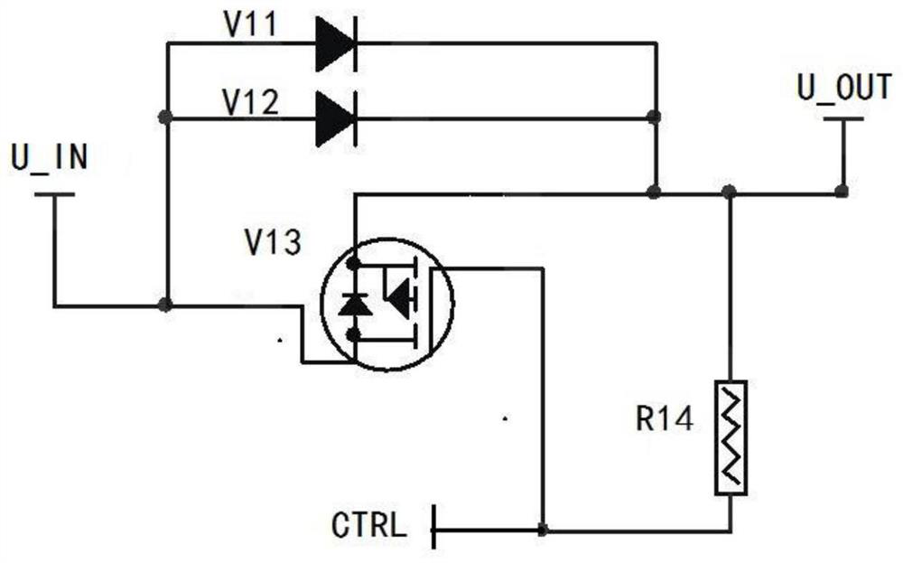
[0028] figure 1 It is a circuit diagram of Embodiment 1. like figure 1 As shown, the voltage self-following anti-backfeed circuit includes a diode V11, a diode V12, a PMOS transistor V13, and a resistor R14; the voltage input terminal U_IN of the voltage self-follower anti-backfeed circuit is connected to the anodes of the diode V11 and the diode V12 and the The drain of the PMOS transistor V13, the voltage self-following voltage output terminal U_OUT of the anti-backfeed circuit is connected to the cathodes of the diode V11 and the diode V12 and the source of the PMOS transistor V13, and the gate of the PMOS transistor V13 Connect the external control signal input terminal CTRL, the external control signal input terminal CTRL can output high and low levels to control the opening and closing of the PMOS transistor V13; one end of the resistor R14 is connected to the source of the PMOS transistor V13, and the other end is connected to the PMOS transistor V13 Gate of V13. As ...

Embodiment approach 2

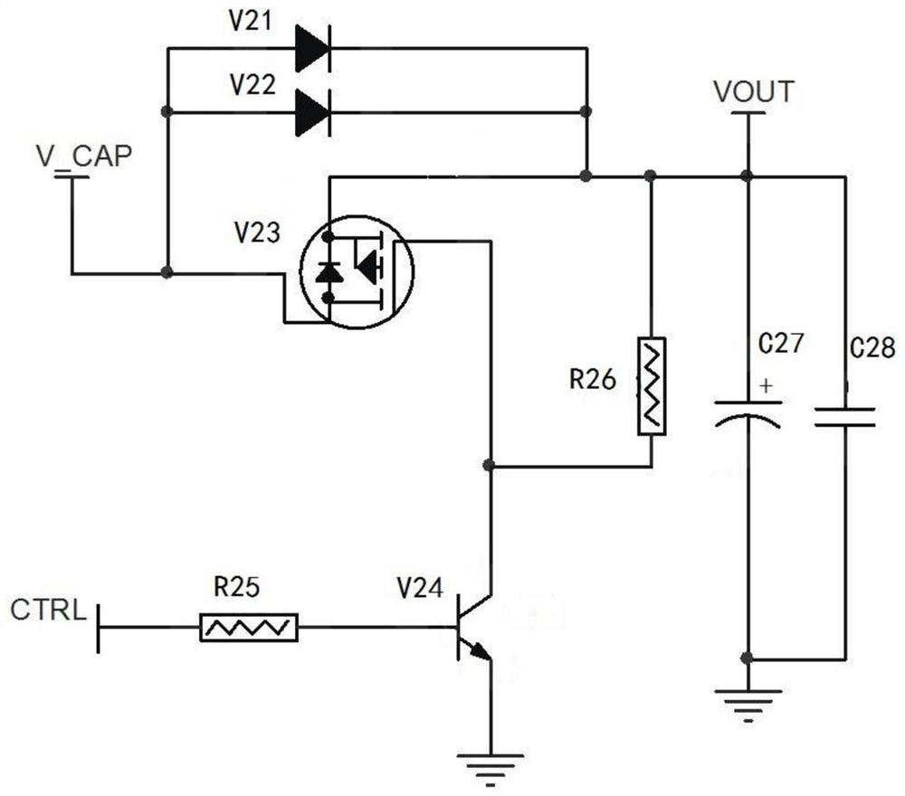
[0033] figure 2 It is a circuit diagram of Embodiment 2 of the present invention. Such as figure 2 As shown, the voltage self-following anti-backfeed circuit includes diode V21, diode V22, PMOS transistor V23, transistor V24, resistor R25, resistor R26, capacitor C27, and capacitor C28; the voltage self-follower anti-backfeed circuit voltage input terminal V_CAP Connect the anodes of the diode V21 and the diode V22 and the drain of the PMOS transistor V23, and connect the voltage output terminal VOUT of the voltage self-following anti-backfeed circuit to the cathodes of the diode V21 and the diode V22 and the PMOS transistor V23 The source of the PMOS transistor V23 is connected to the collector of the transistor V24, one end of the resistor R26 is connected to the source of the PMOS transistor V23, and the other end is connected to the gate of the PMOS transistor V23. The emitter of the transistor V24 is grounded, the base of the transistor V24 is connected to the externa...

Embodiment approach 3

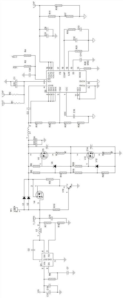
[0036] Figure 4 It is a circuit diagram of Embodiment 3 of the present invention. Such as Figure 4 As shown, the voltage self-following anti-backfeed circuit includes diode V31, diode V32, PMOS transistor V33, MOS transistor V34, resistor R35, resistor R36, capacitor C37, and capacitor C38; the voltage self-follower anti-backfeed circuit voltage input terminal V_CAP is connected to the anode of the diode V31 and the diode V32 and the drain of the PMOS transistor V33, and the voltage output terminal VOUT of the voltage self-following anti-backfeed circuit is connected to the cathode of the diode V31 and the diode V32 and the PMOS transistor the source of V33, the gate of the PMOS transistor V33 is connected to the drain of the MOS transistor V34, one end of the resistor R36 is connected to the source of the PMOS transistor V33, and the other end is connected to the gate of the PMOS transistor V33, The source of the MOS transistor V34 is grounded, the gate of the MOS transis...


PUM


Abstract

The invention relates to a voltage self-following anti-backflow circuit, which comprises N diodes, a PMOS tube and a resistor, the voltage input end of the voltage self-following anti-backflow circuit is connected with the anodes of the N diodes and the drain electrode of the PMOS tube, the voltage output end of the voltage self-following anti-backflow circuit is connected with the cathodes of the N diodes and the source electrode of the PMOS tube, and the grid electrode of the PMOS tube is connected with an external control signal input end. The external control signal input end can output high and low levels to control the on-off of the PMOS tube; one end of the resistor is connected with the source electrode of the PMOS tube, and the other end of the resistor is connected with the grid electrode of the PMOS tube; and the number N of the N diodes is an integer greater than 0. The circuit is applied to a constant-current charging and boost discharging circuit of a battery or a super-capacitor module, reverse charging caused by the fact that leakage current exceeds the standard is prevented, and constant-current charging cut-off voltage and boost discharging voltage can be accurately controlled.

Description

technical field [0001] The invention relates to the technical fields of instruments and meters and intelligent distribution network, in particular to a voltage self-following anti-backfeed circuit. Background technique [0002] In the process of charging the battery or supercapacitor module with constant current, if the input terminal of the constant current DC / DC chip is powered off, and there is a high voltage at the output terminal at this time, there will be a gap between the output of the constant current DC / DC chip and the input. Higher leakage current, if the leakage current is light, it will cause the constant current DC / DC chip to not work normally, such as hiccup-type repeated startup, input and output straight-through, etc., which may lead to abnormal high temperature of the constant current DC / DC chip, chip failure, etc. Burn out, and even the battery or supercapacitor module explodes due to an instant short circuit. Therefore, an anti-backfeed circuit must be i...

Claims


Application Information

Patent Timeline
Patent Type & Authority Applications(China)
IPC IPC(8): G05F1/56
CPCG05F1/561
Inventor 黎毅辉范律肖林松李俊汤可王锋陈岗
Owner WILLFAR INFORMATION TECH CO LTD
Why Eureka
Try Eureka