Selective contact area buried solar cell and back contact structure thereof

A solar cell and back contact technology, applied in the field of solar cells, can solve the problems of high groove width control requirements and poor passivation effect, and solve the problems of poor passivation effect, loose width control requirements, and high width control requirements Effect

Pending Publication Date: 2021-08-24
ZHEJIANG AIKO SOLAR ENERGY TECH CO LTD
View PDF0 Cites 3 Cited by
  • Summary
  • Abstract
  • Description
  • Claims
  • Application Information

AI Technical Summary

Problems solved by technology

[0005] The purpose of the embodiments of the present invention is to provide a back contact structure of a solar...

Method used


Image

  • Selective contact area buried solar cell and back contact structure thereof
  • Selective contact area buried solar cell and back contact structure thereof
  • Selective contact area buried solar cell and back contact structure thereof

Examples


Embodiment 1

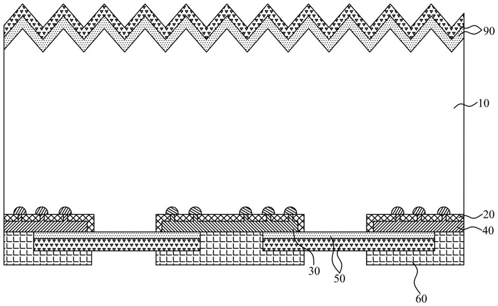
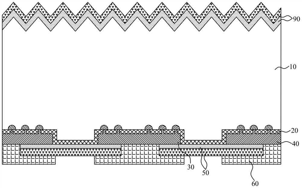
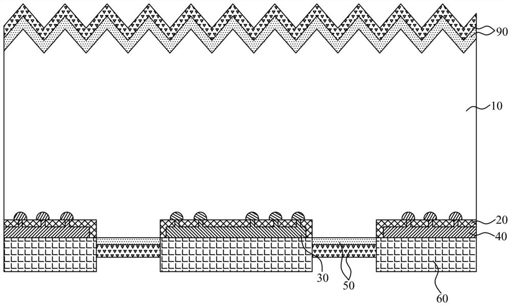
[0080] The first embodiment of the present invention provides a back contact structure of a solar cell. For the convenience of description, only the parts related to the embodiment of the present invention are shown. Refer to Figure 1-Figure 11 As shown, the back contact structure of the solar cell provided by the embodiment of the present invention includes:

[0081] Grooves arranged at intervals on the back side of the silicon substrate 10;

[0082] A first dielectric layer 20 disposed on the back of the silicon substrate 10, the first dielectric layer 20 at least covers the groove;

[0083] P-type doped regions 30 and N-type doped regions 40 arranged on the first dielectric layer 20 and alternately arranged in each groove;

[0084] A second dielectric layer 50 disposed between the P-type doped region 30 and the N-type doped region 40, the second dielectric layer 50 is at least one layer and its refractive index decreases sequentially from the back of the silicon substrate...

Embodiment 2

[0125] The second embodiment of the present invention provides a selective contact area buried solar cell. For the convenience of description, only the parts related to the embodiment of the present invention are shown. Refer to Figure 1-Figure 11 As shown, the selective contact area buried solar cell provided by the embodiment of the present invention includes:

[0126] silicon substrate 10;

[0127] The back contact structure described in the foregoing embodiments on the back side of the silicon substrate 10; and

[0128] The third dielectric layer 90 is disposed on the front surface of the silicon substrate 10 .

[0129] Further, in an embodiment of the present invention, the second dielectric layer 50 and the third dielectric layer 90 can be prepared by preparing the front and back sides of the silicon substrate 10 respectively through the same process, and at this time, the third dielectric layer 90 can be The structure is the same as that of the second dielectric laye...

Embodiment 3

[0136] The third embodiment of the present invention provides a method for fabricating a selective contact region buried solar cell. For the convenience of description, only the parts related to the embodiment of the present invention are shown. Refer to Figure 12 As shown, the selective contact region buried solar cell manufacturing method provided in the embodiment of the present invention is used to prepare the selective contact region buried solar cell as described in the foregoing embodiments. Specifically, the method includes:

[0137] Step S11, creating a plurality of grooves arranged at intervals on the back surface of the silicon substrate;

[0138] Wherein, before step S11, it should also include preprocessing the silicon substrate;

[0139] The above pretreatment includes cleaning the silicon substrate and removing the damaged layer. Specifically, including:

[0140] (1) RCA standard cleaning, remove particles and organic matter on the surface of the silicon subs...


PUM

PropertyMeasurementUnit
Thicknessaaaaaaaaaa
Thicknessaaaaaaaaaa
Thicknessaaaaaaaaaa

Abstract

The invention is suitable for the technical field of solar cells, and provides a selective contact area buried solar cell and a back contact structure thereof. The back contact structure comprises grooves arranged on the back of a silicon substrate at intervals; a first dielectric layer, arranged on the back surface of the silicon substrate and at least covers the groove; P-type doped regions and N-type doped regions arranged on the first dielectric layer and alternately arranged in the grooves; a second dielectric layer arranged between the P-type doped region and the N-type doped region, and the number of the second dielectric layer being at least one; and a conductive layer disposed on the P-type doped region and the N-type doped region. According to the back contact structure provided by the invention, the problems of high control requirement on the width of the groove and poor passivation effect in the prior art are solved.

Description

technical field [0001] The invention belongs to the technical field of solar cells, in particular to a selective contact region buried solar cell and its back contact structure. Background technique [0002] In crystalline silicon solar cells, the efficiency loss of the cell can be divided into two aspects: electrical loss and optical loss. Shielding of surface metal grid lines. [0003] Among them, the passivated metal contact structure has remarkable electrical properties, and can obtain low contact resistivity and low surface recombination at the same time. This structure consists of an ultra-thin tunnel oxide layer and N-type doped or P-type doped polysilicon layer. . Since the light absorption of the doped polysilicon layer is a "parasitic" absorption, that is, it does not contribute to the photo-generated current, so the passivated metal contact structure is mostly used on the back of the cell, so that the front surface can completely avoid the shielding of the metal...

Claims


Application Information

Patent Timeline
IPC IPC(8): H01L31/0224H01L31/0216H01L31/0352H01L31/056H01L31/068H01L31/18
CPCH01L31/022441H01L31/02167H01L31/02168H01L31/035272H01L31/056H01L31/0682H01L31/1804H01L31/1868Y02E10/52H01L31/0747H01L31/035281Y02E10/547H01L31/022466H01L31/02363H01L31/028
Inventor 邱开富王永谦杨新强陈刚
Owner ZHEJIANG AIKO SOLAR ENERGY TECH CO LTD
Why Eureka
Try Eureka