Solar cell and contact structure thereof, cell assembly and photovoltaic system

A solar cell and contact structure technology, applied in the field of solar cells, can solve the problems of complex doping polysilicon process, high process difficulty, expensive equipment, etc., and achieve the effect of avoiding high temperature diffusion process, good deposition effect and low cost

Pending Publication Date: 2021-11-02
ZHEJIANG AIKO SOLAR ENERGY TECH CO LTD +3
View PDF0 Cites 0 Cited by
  • Summary
  • Abstract
  • Description
  • Claims
  • Application Information

AI Technical Summary

Problems solved by technology

[0006] The purpose of the embodiments of the present invention is to provide a contact structure of a solar cell, aiming at solving the difficulty in the existing process of separa

Method used


Image

  • Solar cell and contact structure thereof, cell assembly and photovoltaic system
  • Solar cell and contact structure thereof, cell assembly and photovoltaic system
  • Solar cell and contact structure thereof, cell assembly and photovoltaic system

Examples


Embodiment 1

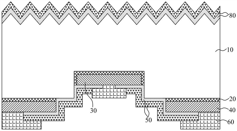
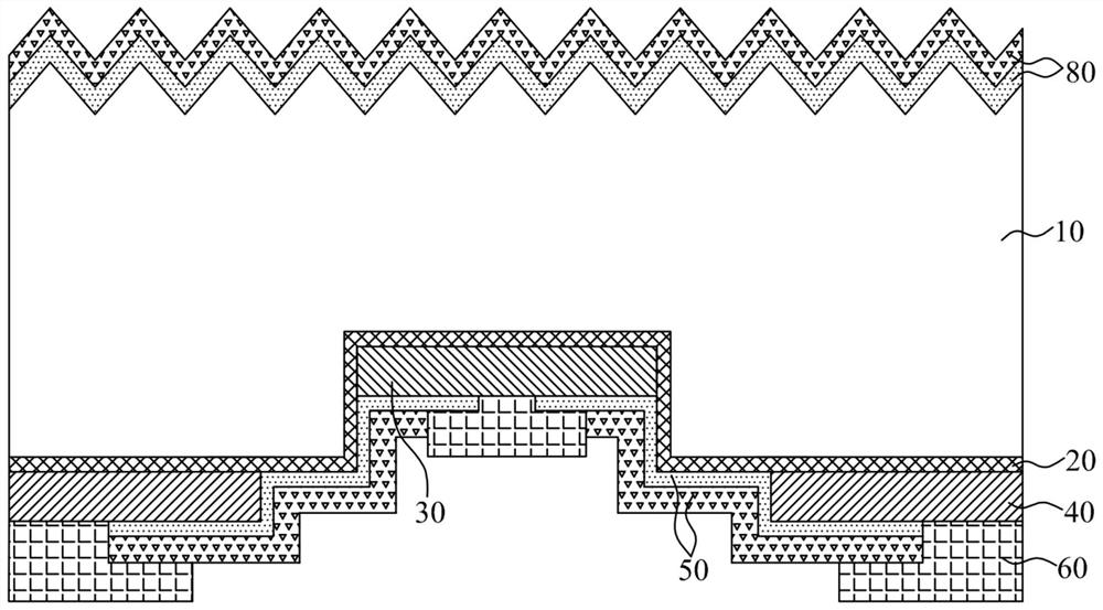
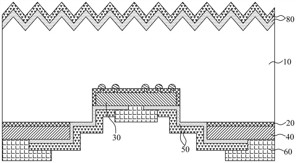
[0075] The embodiment of the present invention provides a contact structure of a solar cell. For the convenience of description, only the parts related to the embodiment of the present invention are shown. Refer to Figure 1 to Figure 11 As shown, the contact structure of the solar cell provided by the embodiment of the present invention includes:

[0076] Grooves arranged at intervals on the back side of the silicon substrate 10;

[0077] A first dielectric layer 20 disposed on the back side of the silicon substrate 10;

[0078] a first selective contact region 30 disposed on the first dielectric layer 20 and disposed in the groove;

[0079] a second selective contact region 40 disposed on the first dielectric layer 20 and disposed outside the groove;

[0080] a second dielectric layer 50 disposed between the first selective contact region 30 and the second selective contact region 40, the second dielectric layer 50 being at least one layer; and

[0081] a conductive layer ...

example 2

[0093] Therefore, in the example in which the hole selective contact region and the electron selective contact region are both non-silicon contact layers, it also includes Example 1: the first selective contact region 30 disposed in the groove is a non-silicon contact layer. The hole selective contact region of the layer, the second selective contact region 40 arranged outside the groove is an electron selective contact region using a non-silicon contact layer; and Example 2: the first selective contact region arranged in the groove The region 30 is an electron selective contact region using a non-silicon contact layer, and the second selective contact region 40 disposed outside the groove is a hole selective contact region using a non-silicon contact layer.

example 3 no. 1 30P, no. 2 40; and example 4

[0094] A specific example in which one of the above-mentioned ones is a non-silicon contact layer and the other is a silicon-based contact layer can be that the hole selective contact region is a non-silicon contact layer, and at this time, the electron selective contact region is a silicon-based contact layer. layer, for example specifically N-type doped polysilicon; or the hole selective contact region is a silicon-based contact layer, for example specifically P-type doped polysilicon, and in this case the electron selective contact region is a non-silicon contact layer. Therefore, it includes Example 1: the first selective contact region 30 arranged in the groove is a hole selective contact region using a non-silicon contact layer, and the second selective contact region 40 arranged outside the groove is a hole selective contact region using an N-type contact layer. Electron selective contact region doped with polysilicon; Example 2: The first selective contact region 30 arr...


PUM

PropertyMeasurementUnit
Work functionaaaaaaaaaa
Thicknessaaaaaaaaaa

Abstract

The invention is suitable for the technical field of solar cells, and provides a solar cell and a contact structure thereof, a cell module and a photovoltaic system. The contact structure comprises grooves arranged at the back of a silicon substrate at intervals, a first dielectric layer which is arranged on the back surface of the silicon substrate, a first selective contact region disposed on the first dielectric layer and disposed within the groove and a second selective contact region disposed outside the groove, a second dielectric layer disposed between the first selective contact region and the second selective contact region, and a conductive layer disposed on the first selective contact region and the second selective contact region. At least one of the first selective contact region and the second selective contact region is a non-silicon contact layer and one is a hole selective contact region and the other is an electron selective contact region. According to the contact structure provided by the invention, the problems of high process difficulty, complex process, expensive equipment and high energy consumption in the existing doped polycrystalline silicon preparation process are solved.

Description

technical field [0001] The invention belongs to the technical field of solar cells, and in particular relates to a solar cell and its contact structure, a cell component and a photovoltaic system. Background technique [0002] In crystalline silicon solar cells, the efficiency loss of the cell can be divided into two aspects: electrical loss and optical loss. Shielding of surface metal grid lines. [0003] Among them, the passivated metal contact structure has remarkable electrical properties, and can simultaneously obtain low contact resistivity and low surface recombination. This structure consists of an ultra-thin tunnel oxide layer and a doped polysilicon layer (P-type or N-type). Since the light absorption of the doped polysilicon layer is parasitic, that is, it does not contribute to the photocurrent, so the passivated metal contact structure is mostly used on the back of the battery, so that the front surface of the battery can completely avoid the shielding of metal...

Claims


Application Information

Patent Timeline
IPC IPC(8): H01L31/0224H01L31/0216H01L31/0236H01L31/054H01L31/02
CPCH01L31/02167H01L31/0547H01L31/02363H01L31/02008H01L31/022441Y02E10/50Y02E10/52
Inventor 邱开富林文杰王永谦杨新强陈刚
Owner ZHEJIANG AIKO SOLAR ENERGY TECH CO LTD
Why Eureka
Try Eureka