Semiconductor structure and manufacturing method thereof

A manufacturing method and semiconductor technology, applied in semiconductor/solid-state device manufacturing, semiconductor devices, transistors, etc., can solve the problems of DRAM manufacturing process difficulty, performance needs to be further improved, and DRAM feature size is small, so as to shorten product production cycle, The effect of avoiding adverse effects and reducing production difficulty

Active Publication Date: 2021-06-29
CHANGXIN MEMORY TECH INC
View PDF9 Cites 1 Cited by
  • Summary
  • Abstract
  • Description
  • Claims
  • Application Information

AI Technical Summary

Problems solved by technology

[0003]However, in order to improve the integration of semiconductor integrated circuits, the feature size of DRAM is getting smaller and smaller; thus making the manu

Method used


Image

  • Semiconductor structure and manufacturing method thereof
  • Semiconductor structure and manufacturing method thereof
  • Semiconductor structure and manufacturing method thereof

Examples


Embodiment Construction

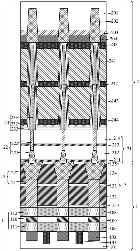
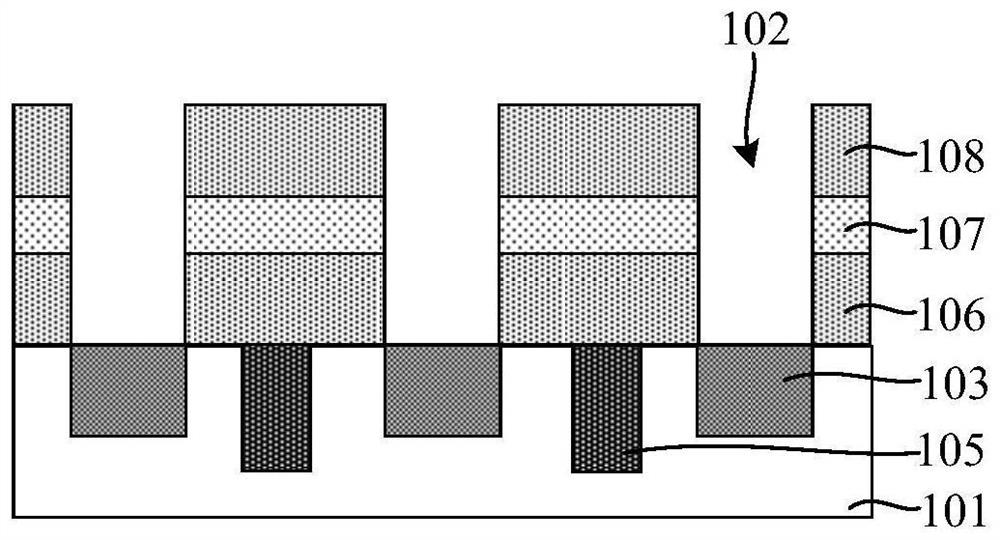
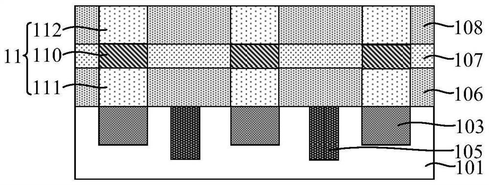
[0033] It can be seen from the background art that the manufacturing process of DRAM is becoming more and more difficult, the production cycle is getting longer and longer, and its performance needs to be further improved. After analysis, it is found that the main reason is that the transistors and capacitors of DRAM are usually formed sequentially on one substrate. However, as the size of DRAM continues to shrink, the process difficulty continues to increase and the production time continues to increase.

[0034] In order to solve the above problems, an embodiment of the present invention provides a semiconductor structure, the semiconductor structure includes: a first substrate, and a second substrate bonded to the first substrate, and the manufacturing process can be performed on the first substrate and the second substrate On, so can shorten the product production cycle. In addition, the first contact structure has a first surface facing the second substrate and a second s...


PUM


Abstract

The embodiment of the invention provides a semiconductor structure and a manufacturing method thereof. The semiconductor structure comprises a first substrate which comprises a bit line, a transistor and a first contact structure which are stacked, and a second substrate which is bonded with the first substrate, and comprises a second contact structure and a capacitor which are stacked, wherein the second contact structure is in direct contact with the first contact structure; the first contact structure is provided with a first surface facing the second substrate and a second surface opposite to the first surface, and the area of the first surface is larger than that of the second surface; and the second contact structure has a third surface facing the first substrate and a fourth surface opposite to the third surface, and the area of the third surface is larger than that of the fourth surface. According to the embodiment of the invention, the manufacturing process difficulty of the DRAM can be reduced, the production cycle is shortened, and the performance of the DRAM is improved.

Description

technical field [0001] Embodiments of the present invention relate to the field of semiconductors, and in particular to a semiconductor structure and a manufacturing method thereof. Background technique [0002] A dynamic random access memory (Dynamic Random Access Memory, DRAM for short) in a semiconductor structure is a semiconductor memory widely used in computer systems. The main working principle of DRAM is to use the amount of charge stored in the capacitor to represent whether a binary bit (bit) is 1 or 0. [0003] However, in order to improve the integration of semiconductor integrated circuits, the feature size of DRAM is getting smaller and smaller; thus making the manufacturing process of DRAM more and more difficult, the production cycle is getting longer and longer, and its performance needs to be further improved. Contents of the invention [0004] Embodiments of the present invention provide a semiconductor structure and a manufacturing method thereof, so a...

Claims


Application Information

Patent Timeline
IPC IPC(8): H01L27/108H01L21/8242
CPCH10B12/30H10B12/02H10B12/033H01L28/90H10B12/315H10B12/05H10B12/482H10B12/488
Inventor 郭帅
Owner CHANGXIN MEMORY TECH INC
Why Eureka
Try Eureka