Selective contact area buried solar cell and back contact structure thereof

A solar cell and back contact technology, applied in the field of solar cells, can solve the problems of high trench width control requirements and poor passivation effect, and achieve the effects of good internal back reflection effect, loose width control requirements, and good passivation effect.

Pending Publication Date: 2021-08-24
ZHEJIANG AIKO SOLAR ENERGY TECH CO LTD
View PDF0 Cites 0 Cited by
  • Summary
  • Abstract
  • Description
  • Claims
  • Application Information

AI Technical Summary

Problems solved by technology

[0005] The purpose of the embodiments of the present invention is to provide a back contact structure of a solar cell, aiming to solve the existing problems of high requirements for groove width control and poor passivation effect

Method used


Image

  • Selective contact area buried solar cell and back contact structure thereof
  • Selective contact area buried solar cell and back contact structure thereof
  • Selective contact area buried solar cell and back contact structure thereof

Examples


Embodiment 1

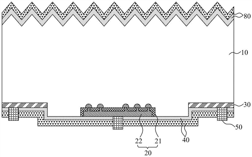
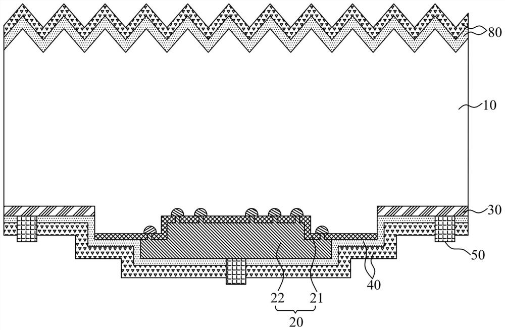
[0087] The first embodiment of the present invention provides a back contact structure of a solar cell, in order to facilitate explanation, only the part related to the embodiment of the present invention, reference Figure 1 - Figure 9 As shown, the back contact structure of the solar cell provided by the embodiment of the present invention includes:

[0088] The spacer is disposed on the recess of the silicon substrate 10;

[0089] Alternately disposed in the first conductive region 20 and the second conductive region 30 in each groove, the first conductive region 20 includes a first dielectric layer 21 and a first doped region 22, a second conductive region disposed sequentially disposed on the recess. 30 includes a second doping region;

[0090] The second dielectric layer 40 is disposed between the first conductive region 20 and the second conductive region 30, the second dielectric layer 40 is at least one layer and is sequentially reduced by the backward refractive index of ...

Embodiment 2

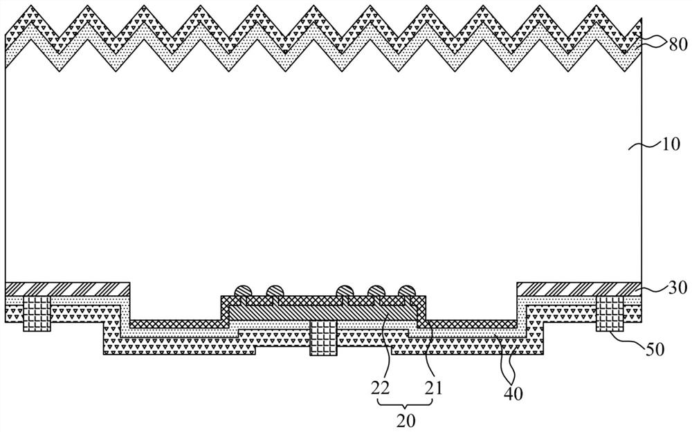
[0130] A second embodiment of the present invention provides a selective contact area buried solar cell, and is shown in order to facilitate explanation, only part of the present invention, referring to Figure 1 - Figure 9 As shown, the selective contact area of ​​the present invention provides the width solar cell including:

[0131] Silicon substrate 10;

[0132] The back contact structure of the foregoing embodiment of the back surface of the silicon substrate 10; and

[0133] The third dielectric layer 80 is provided at the front of the silicon substrate 10.

[0134] Further, in one embodiment of the present invention, its second dielectric layer 40 and the third dielectric layer 80 may be prepared for the front and reverse surface of the silicon substrate 10 by the same process, and the third dielectric layer 80 can be The same as the second dielectric layer 40 in the foregoing embodiment. Thus, according to the foregoing embodiment, the third dielectric layer 80 can also pre...

Embodiment 3

[0141] According to a third embodiment of the present invention, a method of manufacturing a selective contact region buried solar cell, in order to facilitate explanation, only the part related to the embodiment of the present invention, reference Figure 10 As shown, the selective contact region of the present invention is provided by a combined solar cell manufacturing method for preparing a selective contact region, such as the foregoing embodiment, and specific, which comprises:

[0142] Step S11, the plurality of grooves provided at intervals on the back surface of the silicon substrate;

[0143] Among them, in step S11, it should also include pretreatment of silicon substrates;

[0144] The above pretreatment includes cleaning silicon substrates and removing the damage layer. Specific, including:

[0145] (1) RCA standard cleaning, remove particles and organics of the surface of the silicon substrate;

[0146] (2) After the silicon substrate is cleaned, it is then placed in ...


PUM

PropertyMeasurementUnit
thicknessaaaaaaaaaa
thicknessaaaaaaaaaa
thicknessaaaaaaaaaa

Abstract

The invention is suitable for the technical field of solar cells, and provides a selective contact area buried solar cell and a back contact structure thereof. The back contact structure comprises grooves arranged on the back of a silicon substrate at intervals; first conductive regions and second conductive regions alternately arranged in the grooves, each first conductive region comprising a first dielectric layer and a first doped region which are sequentially arranged on the corresponding groove, and each second conductive region comprising a second doped region; a second dielectric layer arranged between the first conductive region and the second conductive region, and the number of the second dielectric layer being at least one; and a conductive layer disposed on the first conductive region and the second conductive region. According to the back contact structure provided by the invention, the problems of high control requirement on the width of the groove and poor passivation effect in the prior art are solved.

Description

Technical field [0001] The invention belongs to the field of solar cell technology, and more particularly to a selective contact region buried solar cell and a back contact structure thereof. Background technique [0002] In crystalline silicon solar cells, the efficiency loss of the battery can be divided into two aspects of electrical loss and optical loss, and an important part of the electrical loss is a composite loss and resistance loss caused by metal-semiconductor contact, and an important part of optical loss is light. The mask of the metal gate line. [0003] The passivation metal contact structure has significant electrical properties, which can simultaneously obtain low contact resistivity and low surface composite, which consists of a layer of ultra-thin tunneling layer and N-type doped or p-doped polysilicon layer. . Since the doped polysilicon layer is absorbed by the absorption of light, that is, the passive current is not contributed, the passivation metal contac...

Claims


Application Information

Patent Timeline
Patent Type & Authority Applications(China)
IPC IPC(8): H01L31/0224H01L31/0216H01L31/0352H01L31/056H01L31/068H01L31/18
CPCH01L31/022441H01L31/02167H01L31/02168H01L31/035272H01L31/056H01L31/0682H01L31/1804H01L31/1868Y02E10/547Y02E10/52H01L31/0747H01L31/035281H01L31/022466H01L31/02363H01L31/028
Inventor 邱开富王永谦杨新强陈刚
Owner ZHEJIANG AIKO SOLAR ENERGY TECH CO LTD
Why Eureka
Try Eureka