Solar cell and preparation method thereof
A technology for solar cells and conductive regions, applied in the field of solar cells, which can solve the problems of poor preparation of hard masks and high requirements for groove width control, and achieve the effects of simple alignment, loose width control requirements, and reduced impurity pollution
- Summary
- Abstract
- Description
- Claims
- Application Information
AI Technical Summary
Problems solved by technology
Method used
Image
Examples
Embodiment 1
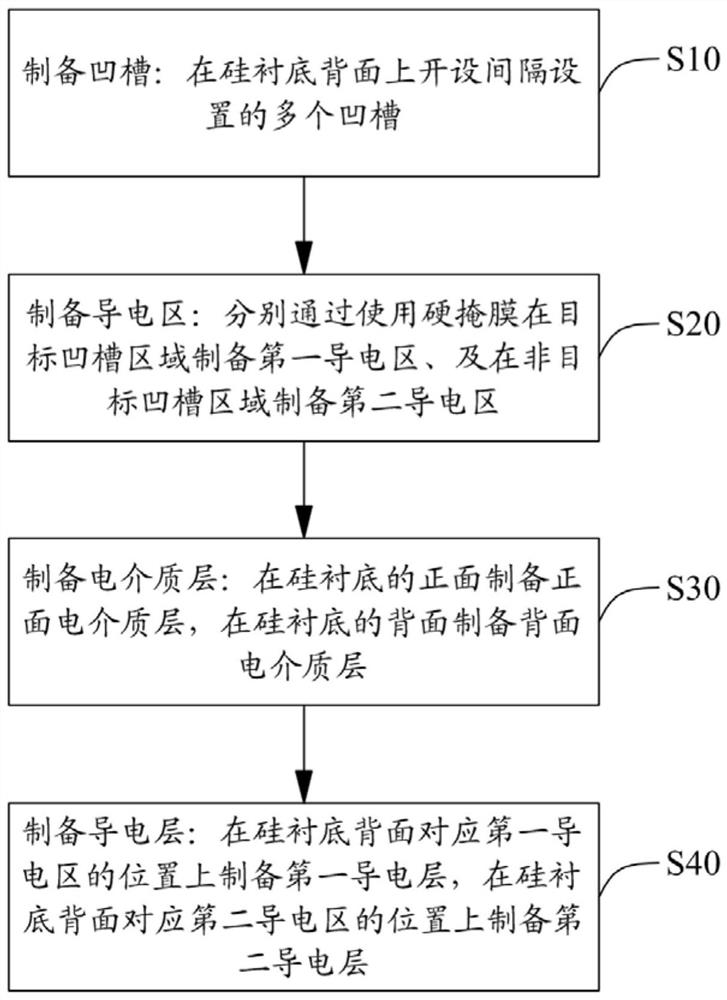
[0051] The first embodiment of the present invention provides a solar cell manufacturing method. For the convenience of description, only the parts related to the embodiment of the present invention are shown. Refer to figure 1 As shown, the solar cell preparation method provided by the embodiment of the present invention includes:
[0052] Step S10, preparing grooves: opening a plurality of grooves arranged at intervals on the back surface of the silicon substrate;
[0053] Wherein, before step S10, it should also include preprocessing the silicon substrate;
[0054] The above pretreatment includes cleaning the silicon substrate and removing the damaged layer. Specifically, including:
[0055] (1) RCA standard cleaning, remove particles and organic matter on the surface of the silicon substrate;
[0056] (2) After the silicon substrate is cleaned, put it into 2-5% KOH alkali solution (potassium hydroxide) or TMAH solution (tetramethylammonium hydroxide, ie developer), the ...
Embodiment 2
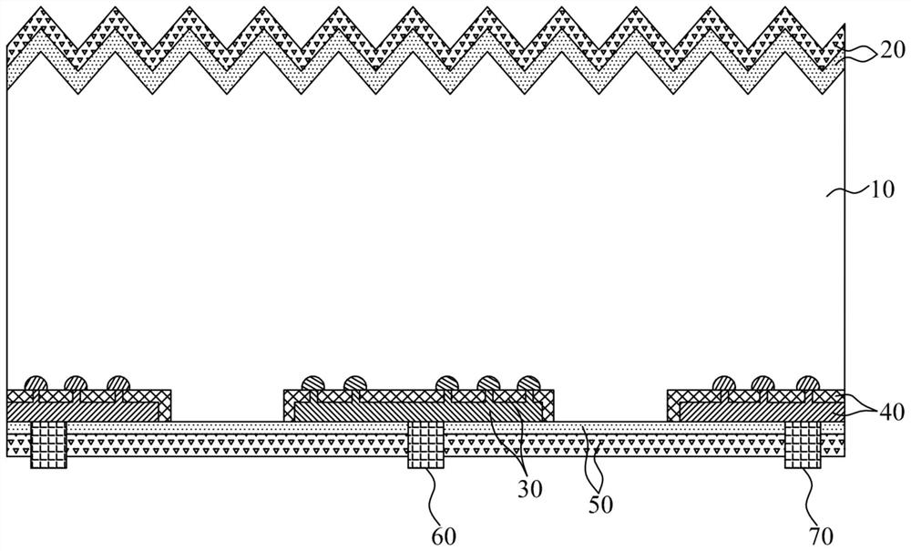
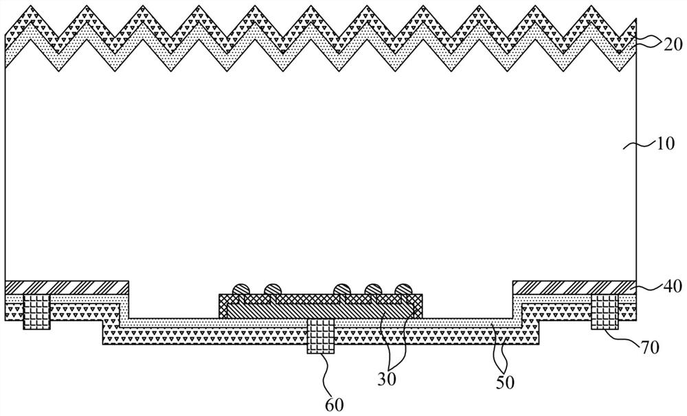
[0118] The second embodiment of the present invention provides a solar cell. For the convenience of description, only the parts related to the embodiment of the present invention are shown. Refer to Figure 2-Figure 8 As shown, the solar cell provided by the embodiment of the present invention includes:
[0119] A silicon substrate 10, the back of the silicon substrate 10 is provided with grooves arranged at intervals;
[0120] A front dielectric layer 20 disposed on the front side of the silicon substrate 10;
[0121] The first conductive region 30 in the target groove region and the second conductive region 40 in the non-target groove region are arranged on the back side of the silicon substrate 10, and the non-target groove region is the land area between each groove or the In the groove region adjacent to the target groove region, the first conductive region 30 and the second conductive region 40 include a passivation contact structure composed of a tunneling layer and a ...
PUM
| Property | Measurement | Unit |
|---|---|---|
| thickness | aaaaa | aaaaa |
Abstract
Description
Claims
Application Information
 - R&D
- Intellectual Property
- Life Sciences
- Materials
- Tech Scout
- Unparalleled Data Quality
- Higher Quality Content
- 60% Fewer Hallucinations
Browse by: Latest US Patents, China's latest patents, Technical Efficacy Thesaurus, Application Domain, Technology Topic, Popular Technical Reports.
© 2025 PatSnap. All rights reserved.Legal|Privacy policy|Modern Slavery Act Transparency Statement|Sitemap|About US| Contact US: help@patsnap.com


