Optical circuit, optical signal processing method and device and readable storage medium

A processing method and storage medium technology, applied in the fields of electrical digital data processing, optics, nonlinear optics, etc., can solve the problems of inability to achieve fast processing, huge computing system, and no use of implementation, and achieve faster convolution calculation speed, simplifying Optical device structure, effect of number reduction

Active Publication Date: 2021-08-31
山东云海国创云计算装备产业创新中心有限公司
View PDF8 Cites 1 Cited by
  • Summary
  • Abstract
  • Description
  • Claims
  • Application Information

AI Technical Summary

Problems solved by technology

No matter it takes a lot of time to achieve fast processing efficiency, and superimposed a large number of MZI devices, it will make the overall computing system huge and complex.

Method used


Image

  • Optical circuit, optical signal processing method and device and readable storage medium
  • Optical circuit, optical signal processing method and device and readable storage medium
  • Optical circuit, optical signal processing method and device and readable storage medium

Examples


Embodiment Construction

[0054] In order to enable those skilled in the art to better understand the solution of the present application, the present application will be further described in detail below in conjunction with the drawings and specific implementation methods. Apparently, the described embodiments are only some of the embodiments of this application, not all of them. Based on the embodiments in this application, all other embodiments obtained by persons of ordinary skill in the art without making creative efforts belong to the scope of protection of this application.

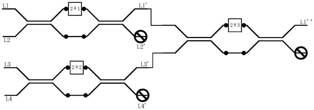
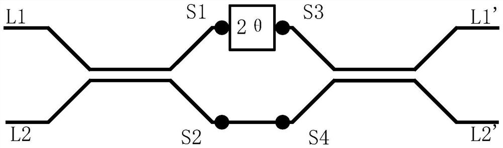
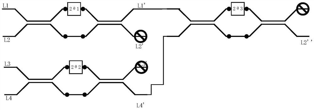
[0055] Please refer to figure 1 , figure 1 It is a schematic diagram of an optical circuit in the embodiment of the present application, and the optical circuit includes:

[0056] An optical output end of the first MZI is connected to an optical input end of the third MZI;

[0057] One optical output end of the second MZI is connected to another optical input end of the third MZI;

[0058] The two optical input terminal...


PUM


Abstract

The invention discloses an optical circuit, an optical signal processing method, an optical signal processing device, optical signal processing equipment and a readable storage medium. The optical circuit is characterized in that one optical output end of a first MZI is connected with one optical input end of a third MZI; one optical output end of the second MZI is connected with the other optical input end of the third MZI; two optical input ends of the first MZI and two optical input ends of the second MZI are respectively connected with optical signals corresponding to a 2*2 convolution sequence to be multiplied; the first MZI, the second MZI and the third MZI respectively carry out phase shift on input optical signals of the first MZI, the second MZI and the third MZI so as to realize convolution calculation; and one optical output end of the third MZI outputs a light signal carrying a convolution result. According to the optical circuit, the number of MZIs is smaller, and a structure is simpler; compared with 2*2 convolution operation achieved in a Gridnet mode, half of time loss and equipment loss can be saved, a convolution calculation speed can be increased, and the structure of an optical device can be simplified.

Description

technical field [0001] The present application relates to the field of computer application technology, in particular to an optical circuit, an optical signal processing method, device and readable storage medium. Background technique [0002] In recent years, people's demand for optical computing technology has increased rapidly. Optical computing can be divided into analog optical computing and digital optical computing. One of the most typical examples of analog light calculations is Fourier operations, which require the use of Fourier transform-related calculations, such as convolution calculations, in areas such as image processing. Using a traditional computer to calculate the Fourier transform is very computationally intensive, and the process of light passing through the lens itself is a Fourier transform process, which takes almost no time at all. Digital optical computing uses the combination of light and optical devices to form classic logic gates, constructs a ...

Claims


Application Information

Patent Timeline
IPC IPC(8): G02F1/21G06F17/15G06F17/14
CPCG02F1/21G06F17/15G06F17/141
Inventor 吴睿振王凛
Owner 山东云海国创云计算装备产业创新中心有限公司
Why Eureka
Try Eureka