Semiconductor Process Method

A process method and semiconductor technology, applied in the direction of semiconductor devices, semiconductor/solid-state device parts, semiconductor/solid-state device testing/measurement, etc., can solve the problems of difficult to identify the direction of the wafer cut, prone to errors, and identify the wafer. , to achieve the effect of improving the level of quality management

Active Publication Date: 2022-06-21
SIEN QINGDAO INTEGRATED CIRCUITS CO LTD
View PDF9 Cites 0 Cited by
  • Summary
  • Abstract
  • Description
  • Claims
  • Application Information

AI Technical Summary

Problems solved by technology

In the prior art, the backside of the wafer is usually photographed after the ink pass die is completed, and the positions of the defective chips on the picture are fitted to the front side of the wafer, and then cut according to the fitting result. However, due to the optical and image Due to various reasons such as depth scaling, errors are prone to occur in this process, and all defective chips cannot be correctly identified.
Specifically, optical reasons include unexpected offset during the photographing process, shadows caused by foreign objects, optical reflections, etc., or the color of the wafer is similar to the background and it is difficult to identify the wafer from the background, or it is difficult to identify the wafer The direction of the kerf, etc.; and the problem in the process of image depth scaling is usually due to the problem of the shooting angle that the captured wafer image is usually ellipsoidal, and it is difficult to reconstruct the defects on the wafer based on the ellipsoidal wafer image.

Method used


Image

  • Semiconductor Process Method
  • Semiconductor Process Method
  • Semiconductor Process Method

Examples


Embodiment Construction

[0034] The embodiments of the present invention are described below through specific specific examples, and those skilled in the art can easily understand other advantages and effects of the present invention from the contents disclosed in this specification. The present invention can also be implemented or applied through other different specific embodiments, and various details in this specification can also be modified or changed based on different viewpoints and applications without departing from the spirit of the present invention.

[0035] see Figure 1 to Figure 5 . It should be noted that the drawings provided in this embodiment are only to illustrate the basic concept of the present invention in a schematic way, although the drawings only show the components related to the present invention rather than the number, shape and the number of components in actual implementation. For dimension drawing, the type, quantity and proportion of each component can be changed at ...


PUM


Abstract

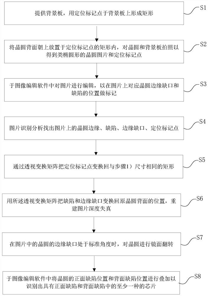
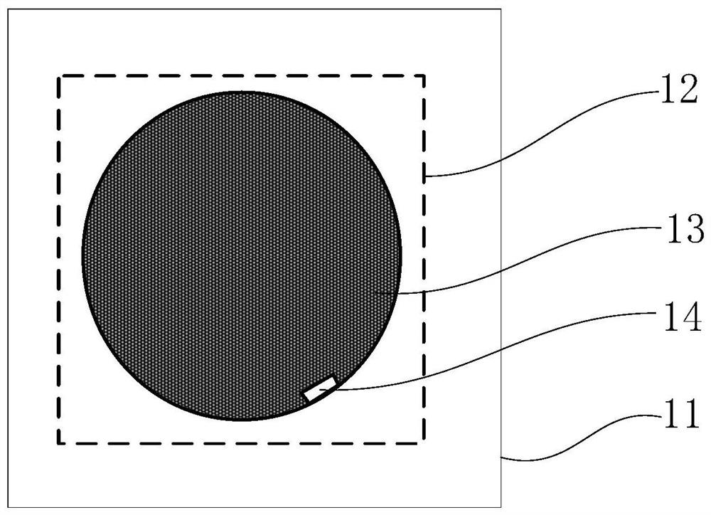
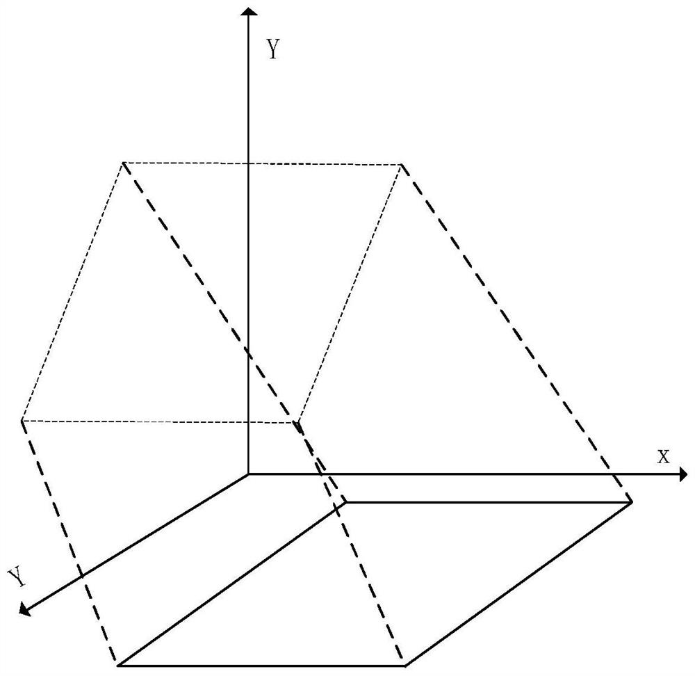
The invention provides a semiconductor process method, comprising the steps of: 1) providing a background plate, and forming a rectangle on the background plate with positioning mark points; Oval wafer picture and positioning mark points; 3) Edit the picture to mark the positions corresponding to wafer edge notches and defects; 4) Find the wafer edge, defects, edge notches, and positioning mark points on the picture ; 5) transform the positioning mark point back to a rectangle with the same size as step 1); 6) transform the defects and edge gaps back to the position on the back of the original wafer, and reconstruct the depth distortion of the picture; 7) carry out mirror flipping on the wafer; 8) The front-side defect locations and the back-side defect locations of the wafer are overlaid to identify chips having at least one of the front-side defects and the back-side defects. The invention helps to accurately reflect the defects on the back side of the wafer to the front side of the wafer so as to accurately detect all defective chips.

Description

technical field [0001] The invention relates to the field of semiconductor chip manufacturing, in particular to a semiconductor process method. Background technique [0002] A final inspection of the wafer is usually performed before the wafer is diced to separate the wafer into individual chips, in which the chips exhibit poor reliability or poor reliability due to surface scratches, particle contamination, etc. For other defects, it is necessary to mark the defective chip, which is usually called an "ink pass die" process. Defects on either of the front and back surfaces of the wafer corresponding to the same chip need to be marked. Therefore, the backside defects of the wafer are reflected to the front side of the wafer, so as to determine all the defects based on the front and backside defects of the wafer The location of the defective chip is very important. In the prior art, the back of the wafer is usually photographed after the ink pass die is completed, and the po...

Claims


Application Information

Patent Timeline
Patent Type & Authority Patents(China)
IPC IPC(8): H01L21/66H01L23/544
CPCH01L22/24H01L22/30
Inventor 林光启陈真刘晨旭邱文莹
Owner SIEN QINGDAO INTEGRATED CIRCUITS CO LTD
Why Eureka
Try Eureka