
Backboard manufacturing method, backboard, display panel and display device

A manufacturing method and display panel technology, applied in semiconductor/solid-state device manufacturing, electrical components, electric solid-state devices, etc., can solve problems such as large seams

Inactive Publication Date: 2021-08-31
上海步哒科技合伙企业(有限合伙)
View PDF0 Cites 1 Cited by
  • Summary
  • Abstract
  • Description
  • Claims
  • Application Information

AI Technical Summary

Problems solved by technology

[0003] Based on this, it is necessary to provide a method for making a backplane that realizes the seamlessness of the splicing screen during the splicing process in view of the problem that the splicing seam of the current splicing screen is too large

Method used


Image

  • Backboard manufacturing method, backboard, display panel and display device
  • Backboard manufacturing method, backboard, display panel and display device
  • Backboard manufacturing method, backboard, display panel and display device

Examples


Embodiment Construction

[0031] In order to make the above-mentioned purpose, features and advantages of the present application more obvious and understandable, the specific implementation manners of the present application will be described in detail below in conjunction with the accompanying drawings. In the following description, numerous specific details are set forth in order to provide a thorough understanding of the application. However, the present application can be implemented in many other ways different from those described here, and those skilled in the art can make similar improvements without departing from the connotation of the present application, so the present application is not limited by the specific embodiments disclosed below.

[0032] In the description of the present application, it should be understood that the terms "center", "longitudinal", "transverse", "length", "width", "thickness", "upper", "lower", "front", " Back", "Left", "Right", "Vertical", "Horizontal", "Top", "...


PUM


Abstract

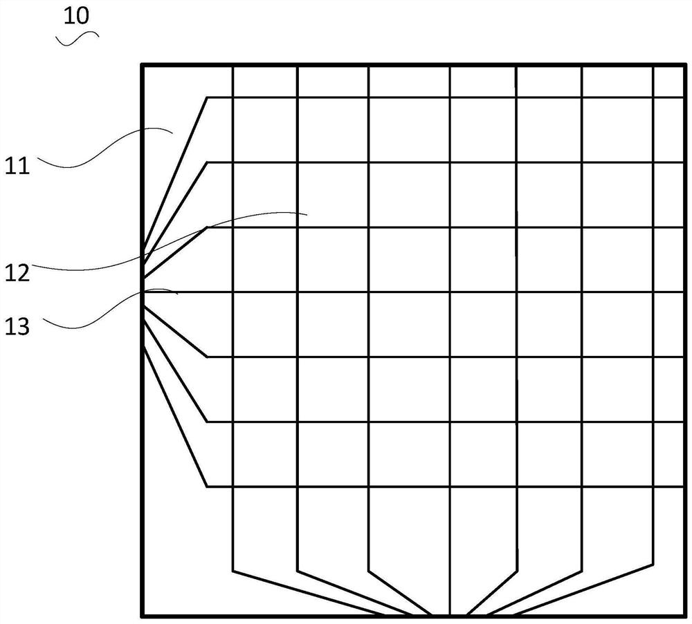
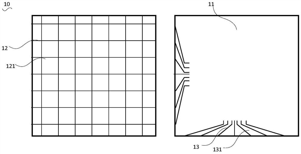
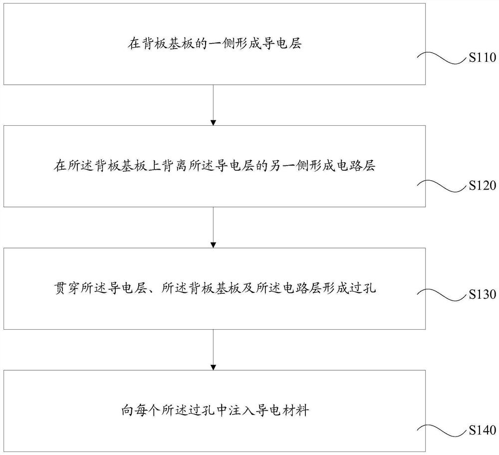
The invention relates to a backboard manufacturing method, a backboard, a display panel and a display device. The backboard manufacturing method comprises the following steps of forming a conductive layer on one side of a backboard substrate, forming a circuit layer on the other side, deviating from the conductive layer, of the backboard substrate, forming via holes in the conductive layer, the backboard substrate and the circuit layer, injecting a conductive material into the via hole, wherein the conductive layer and the circuit layer are electrically connected through the conductive material in the hole. The conductive layer is electrically connected with the circuit layer through the via hole in the backboard substrate below the conductive layer, so that the influence of the wiring area of the binding area on the frame of the display panel can be reduced, and the purpose of reducing the width of the frame of the display panel is achieved. In addition, the influence of wiring in a COF mode on the frame of the display panel can be reduced, and the seamlessness of the spliced screen in the splicing process is achieved. And meanwhile, compared with side surface binding, the requirement on the precision of the side surface of the backboard substrate is lower.

Description

technical field [0001] The present application relates to the field of display technology, in particular to a manufacturing method of a backplane, a backplane, a display panel and a display device. Background technique [0002] In the field of display, such as liquid crystal display (Liquid Crystal Display, LCD), organic light-emitting semiconductor (Organic Light-Emitting Diode, OLED), light-emitting diode (Light Emitting Diode, referred to as LED), micro light-emitting diode (Micro LED) screen, a single The larger the screen body, the higher the production cost (price / area), so a general super large screen is usually formed by splicing several small screens together to reduce the cost per unit area. Since the general screen will have borders, such as figure 1 As shown, this will lead to several non-display dark areas in the display area of ​​the splicing screen, which will reduce the display quality. How to reduce the size of the splicing seam of the splicing screen has ...

Claims


Application Information

Patent Timeline
Patent Type & Authority Applications(China)
IPC IPC(8): H01L21/77H01L27/12
CPCH01L27/124H01L27/1259
Inventor 秦凯
Owner 上海步哒科技合伙企业(有限合伙)
Learn More