
Memory control method and device

A memory control and memory chip technology, applied in the field of communications, can solve problems such as increased interrupt frequency and increased response burden.

Pending Publication Date: 2021-09-07
BEIJING MECHANICAL EQUIP INST
View PDF5 Cites 0 Cited by
  • Summary
  • Abstract
  • Description
  • Claims
  • Application Information

AI Technical Summary

Problems solved by technology

[0005] In view of the above-mentioned analysis, the embodiment of the present invention aims to provide a memory control method and device to solve the problem that when the data bidirectional transmission rate is too high due to the small FPGA cache, the interrupt frequency will also increase accordingly, and the When the upper computer is embedded hardware, because the scheduling cycle of the operating system is generally millisecond level, the high interrupt frequency increases the response burden and other problems.

Method used


Image

  • Memory control method and device
  • Memory control method and device
  • Memory control method and device

Examples


Embodiment Construction

[0031] Preferred embodiments of the present invention will be described in detail below in conjunction with the accompanying drawings, wherein the accompanying drawings constitute a part of the application and together with the embodiments of the present invention are used to explain the principle of the present invention and are not intended to limit the scope of the present invention.

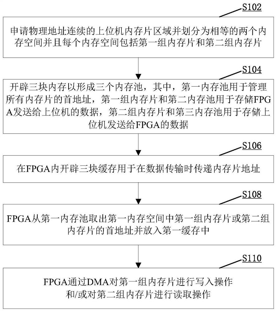
[0032] A specific embodiment of the present invention discloses a memory control method. like figure 1As shown, the memory control method includes: step S102, apply for a host computer memory slice area with continuous physical addresses and divide it into two equal memory spaces and each memory space includes a first group of memory slices and a second group of memory slices; step S104 , open up three pieces of memory to form three memory pools, among which, the first memory pool is used to manage the first address of all memory slices, the first group of memory slices and the second memory ...


PUM


Abstract

The invention relates to a memory control method and device, belongs to the technical field of communication, and solves the problems that in the prior art, due to the fact that the cache of an FPGA is small, when the data two-way transmission rate is too high, the interruption frequency is also increased, and the like. The memory control method comprises the steps that an upper computer memory chip area with continuous physical addresses is applied for and the upper computer memory chip area is divided into two equal memory spaces, wherein each memory space comprises a first group of memory chips and a second group of memory chips; three memories are developed to form three memory pools, and the first memory pool is used for managing initial addresses of all memory pieces; three caches are developed in the FPGA and used for transmitting memory chip addresses during data transmission; the FPGA takes out the first address of the first group of memory chips or the second group of memory chips in the first memory space from the first memory pool and puts the first address into a first cache; and the FPGA performs write-in operation on the first group of memory chips and / or performs read-in operation on the second group of memory chips through the DMA. The interruption frequency of the driving layer of the upper computer is reduced.

Description

technical field [0001] The present invention relates to the field of communication technology, in particular to a memory control method and device. Background technique [0002] Field Programmable Gate Array FPGA (Field Programmable Gate Array) is a product of further development on the basis of programmable devices. It is a semi-custom circuit in the field of application-specific integrated circuits (ASIC). It overcomes the shortcomings of the limited number of gate circuits of the original programmable device. [0003] When FPGA is used for high-speed data acquisition in the industrial field, frequent communication will be performed between FPGA and host computer. The traditional method is to use direct memory access DMA (Direct Memory Access), which allows hardware devices of different speeds to communicate without relying on a large number of interrupt loads of the CPU) to transfer data between the FPGA and the host computer. When the FPGA writes data, when the FPGA ca...

Claims


Application Information

Patent Timeline
Patent Type & Authority Applications(China)
IPC IPC(8): G06F12/02G06F3/06
CPCG06F12/023G06F3/0644G06F3/0647G06F3/061G06F3/0671
Inventor 刘磊
Owner BEIJING MECHANICAL EQUIP INST
Learn More