Press fitting device for assembling semiconductor element

A press-fitting device, semiconductor technology, applied in metal processing, metal processing equipment, manufacturing tools, etc., can solve problems such as affecting semiconductor component processing, chip damage, uneven force, etc.

Inactive Publication Date: 2021-09-10
安徽富信半导体科技有限公司
View PDF8 Cites 1 Cited by
  • Summary
  • Abstract
  • Description
  • Claims
  • Application Information

AI Technical Summary

Problems solved by technology

[0004] The purpose of the present invention is to provide a press-fitting device for semiconductor element assembly, which solves the following technical problems: (1) artificially assisted press-fitting causes semiconductor elements to be stressed unevenly during press-fitting, which easily leads to chip damage; After the combination is completed, it is difficult to remove the semiconductor components manually, which affects the subsequent processing of the semiconductor components

Method used


Image

  • Press fitting device for assembling semiconductor element
  • Press fitting device for assembling semiconductor element
  • Press fitting device for assembling semiconductor element

Examples


Embodiment Construction

[0024] The following will clearly and completely describe the technical solutions in the embodiments of the present invention with reference to the accompanying drawings in the embodiments of the present invention. Obviously, the described embodiments are only some, not all, embodiments of the present invention. Based on the embodiments of the present invention, all other embodiments obtained by persons of ordinary skill in the art without creative efforts fall within the protection scope of the present invention.

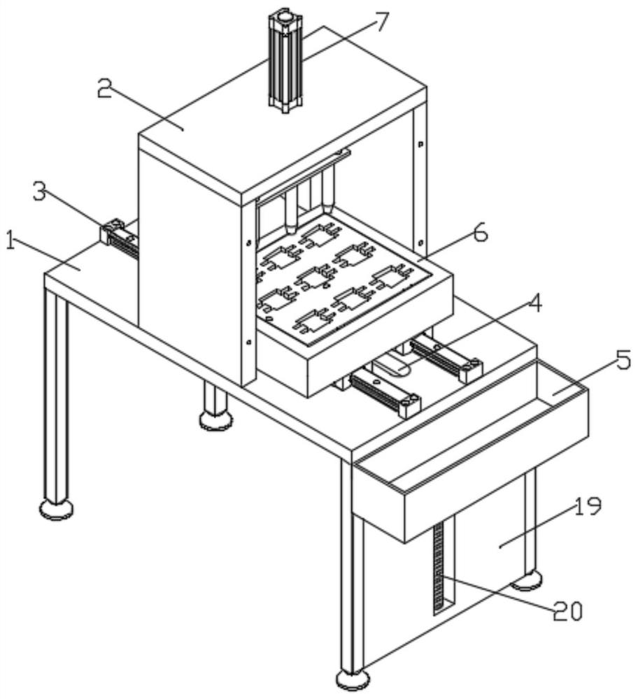
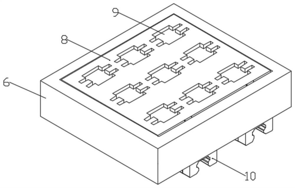
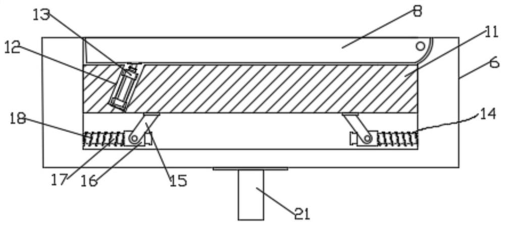
[0025] see Figure 1-5 As shown, the present invention is a press-fitting device for semiconductor element assembly, comprising a carrier 1, a press-fit box 6 is arranged on the top of the carrier 1, and a press-fit plate 8 for storing semiconductor elements is arranged in the press-pack box 6, and the press-fit A plurality of accommodating grooves 9 are provided on the mounting plate 8, and an overturning assembly for driving the pressing plate 8 to turn over is a...


PUM


Abstract

The invention discloses a press fitting device for assembling a semiconductor element. The press fitting device comprises a carrying table, a press fitting box is arranged at the top of the carrying table; a press fitting plate for storing the semiconductor element is arranged in the press fitting box; a plurality of accommodating grooves are formed in the press fitting plate; an overturning assembly for driving the press fitting plate to overturn is arranged in the press fitting box; and buffering assemblies used for buffering the press fitting plate are symmetrically arranged on the two sides of the bottom of the overturning assembly. According to the press fitting device, the press fitting box and a press fitting assembly are arranged, a press fitting roller on the press fitting assembly is matched with the press fitting plate on the press fitting box, and then a cooling fin is effectively pressed to the semiconductor element; and the buffering assemblies are arranged at the bottom of the press fitting plate, buffering springs on the buffering assemblies buffer pressure applied by the press fitting roller, and the damage of the semiconductor element caused by overlarge pressure is avoided, so that the press fitting effect is ensured, meanwhile, the situation that the stress of the semiconductor element is inconsistent due to manual press fitting and the semiconductor element is pressed and damaged is avoided, and the working efficiency is improved.

Description

technical field [0001] The invention relates to the technical field of semiconductor element processing, in particular to a press-fitting device for semiconductor element assembly. Background technique [0002] In order to quickly dissipate the high temperature generated during the operation of the semiconductor element and operate normally at an appropriate operating temperature, in the structure of the semiconductor element, a heat sink is usually pressed on the substrate provided with the semiconductor chip to make the semiconductor element The high temperature generated by the component operation can be conducted to the heat sink, and then the heat dissipation surface area is enlarged through the heat sink to dissipate heat. [0003] However, in the process of laminating semiconductor elements with existing semiconductor element laminating machines, manual assisted pressing is usually used, and the force on both sides above the pressing plate is prone to be inconsistent,...

Claims


Application Information

Patent Timeline
Patent Type & Authority Applications(China)
IPC IPC(8): B23P19/027B23P19/00
CPCB23P19/027B23P19/00
Inventor 周海生蒋振荣
Owner 安徽富信半导体科技有限公司
Why Eureka
Try Eureka