
Thin film based semiconductor devices and methods of forming thin film based semiconductor device

A semiconductor and thin-film technology, applied in the fields of semiconductor devices, semiconductor/solid-state device manufacturing, semiconductor/solid-state device components, etc., and can solve problems such as increasing the complexity of the manufacturing process

Pending Publication Date: 2021-09-10
GLOBALFOUNDRIES SINGAPORE PTE LTD
View PDF4 Cites 0 Cited by
  • Summary
  • Abstract
  • Description
  • Claims
  • Application Information

AI Technical Summary

Problems solved by technology

However, these fabrication processes require additional masks and increase the complexity of the fabrication process

Method used


Image

  • Thin film based semiconductor devices and methods of forming thin film based semiconductor device
  • Thin film based semiconductor devices and methods of forming thin film based semiconductor device
  • Thin film based semiconductor devices and methods of forming thin film based semiconductor device

Examples


Embodiment Construction

[0022] Embodiments described below in the context of the apparatus are similarly valid for the respective methods and vice versa. Furthermore, it should be understood that the embodiments described below may be combined, for example, a part of one embodiment may be combined with a part of another embodiment.

[0023] It should be understood that any attribute described herein for a particular device may also apply to any device described herein. It should be understood that any property described herein for a particular method may also apply to any method described herein. In addition, it should also be understood that for any device or method described herein, not necessarily all described components or steps must be included in the device or method, but only some (but not all) components or steps may be included.

[0024] It should be understood that when the terms "upper", "upper", "top", "bottom", "lower", "side", "back", "left", "right", "front", "Lateral", "upper" and ...


PUM

PropertyMeasurementUnit
thicknessaaaaaaaaaa

Abstract

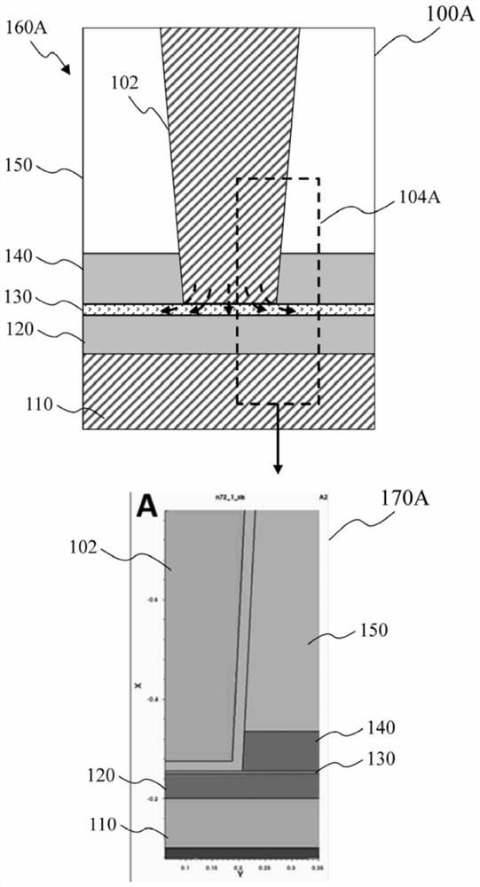
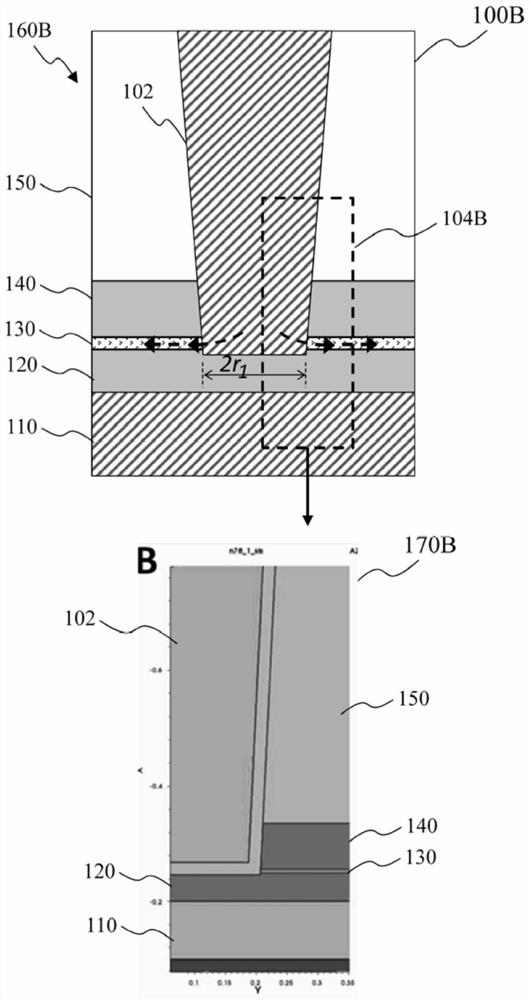
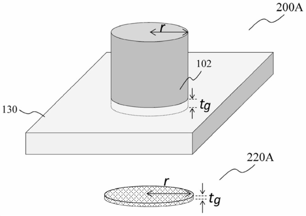
The invention relates to a thin film based semiconductor devices and methods of forming a thin film based semiconductor device. According to various embodiments, a semiconductor device may include a thin film arranged within a first inter-level dielectric layer, a masking region, and a contact plug. The masking region may be arranged over the thin film, within the first inter-level dielectric layer. The masking region may be structured to have a higher etch rate than the first inter-level dielectric layer. The contact plug may extend along a vertical axis, from a second inter-level dielectric layer to the thin film. A bottom portion of the contact plug may be surrounded by the masking region. The bottom portion of the contact plug may include a lateral member that extends along a horizontal plane at least substantially perpendicular to the vertical axis. The lateral member may be in contact with the thin film.

Description

technical field [0001] Various embodiments relate to thin film based semiconductor devices and methods of forming thin film based semiconductor devices. Background technique [0002] Thin film based passive components, such as thin film resistors (TFRs), are used in high precision analog and mixed signal or RF applications. For example, TFRs are primarily used as part of complex integrated circuits to provide high precision resistance in devices with low temperature coefficient of resistance (TCR). Often, special care may be required during the fabrication of such thin film-based devices. For example, the process of contacting the overlying metal interconnect layer and the TFR in a conventional top side via pick-up configuration can lead to breakdown of the TFR when the via is formed, which can result in high contact resistance, Increased in-wafer TCR and high variability resistors. Prior art fabrication processes to prevent breakdown may include forming a buffer layer on...

Claims


Application Information

Patent Timeline
Patent Type & Authority Applications(China)
IPC IPC(8): H01L23/64H01L21/768H10N97/00
CPCH01L28/20H01L21/31116H01L21/32135H01L23/5226H01L23/5228H01L21/76805H01L21/76804H01L23/53295H01L21/76802H01L21/31111H01L21/76877H01L23/528
Inventor 冯陈刚李汉和邵艳霞廖国盛
Owner GLOBALFOUNDRIES SINGAPORE PTE LTD
Learn More