Longitudinal motion platform and electron beam detection equipment with same

A technology of longitudinal movement and detection equipment, applied in the direction of circuits, discharge tubes, electrical components, etc., can solve the problems of image out of focus, low detection efficiency, and less effective detection time

Pending Publication Date: 2021-09-14
ZHONGKE JINGYUAN ELECTRON LTD
View PDF5 Cites 2 Cited by
  • Summary
  • Abstract
  • Description
  • Claims
  • Application Information

AI Technical Summary

Problems solved by technology

The line width of integrated circuits is becoming more and more miniaturized, and higher and more difficult requirements are placed on the production process technology of circuits. Not only must sub-micron lines be etched, but line defects must also be controlled within a certain range to ensure The function and yield of the chip, the traditional optical inspection equipment can no longer meet the needs, and the electron beam inspection equipment overcomes the limitation of the optical wavelength, so that the resolution can be improved to the nanometer field, and extremely small defects can be detected
[0003] In the actual detection process of the electron beam detection equipment, there is a deviation between each scanning point. When the deviation exceeds the range of the electron beam scanning electron microscope's sinking depth, the image detected by the electron beam scanning electron microscope will be out of focus. In order to obtain a clear In the out-of-focus position of the image, the electron beam scanning electron microscope needs to re-autofocus, and a large amount of time is in the autofocus state during detection. The real effective detection time of the equipment is less, resulting in low detection efficiency

Method used


Image

  • Longitudinal motion platform and electron beam detection equipment with same
  • Longitudinal motion platform and electron beam detection equipment with same
  • Longitudinal motion platform and electron beam detection equipment with same

Examples


Embodiment Construction

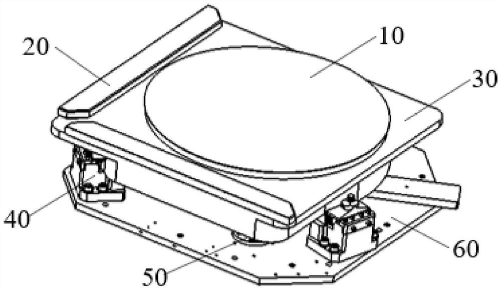
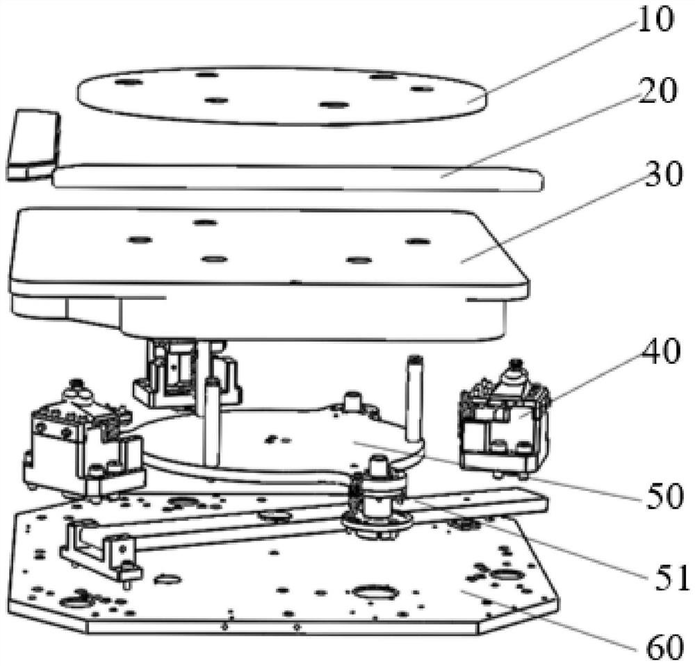
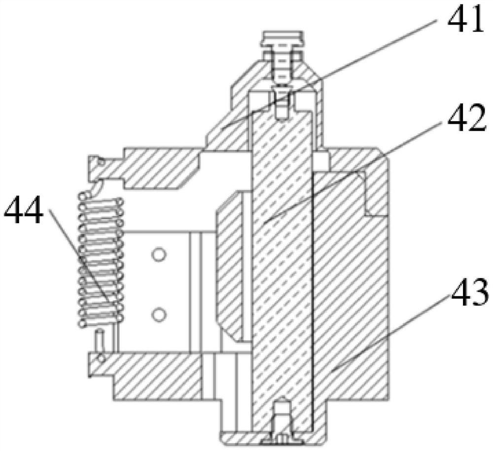
[0031] Various exemplary embodiments, features, and aspects of the present application will be described in detail below with reference to the accompanying drawings. The same reference numbers in the figures indicate functionally identical or similar elements. While various aspects of the embodiments are shown in drawings, the drawings are not necessarily drawn to scale unless specifically indicated.

[0032] Wherein, it should be understood that the terms "center", "longitudinal", "transverse", "length", "width", "upper", "lower", "front", "rear", "left", "right" ", "Vertical", "Horizontal", "Top", "Bottom", "Inner", "Outer", "Clockwise", "Counterclockwise", "Axial", "Radial", "Circumferential ” and other indicated orientations or positional relationships are based on the orientations or positional relationships shown in the drawings, and are only for the convenience of describing the application or simplifying the description, rather than indicating or implying that the ref...


PUM


Abstract

The invention relates to a longitudinal motion platform. The longitudinal motion platform is suitable for being installed in electron beam detection equipment and is characterized by comprising a platform bottom plate, a lifting mechanism, an insulating supporting table and an electrostatic chuck which are sequentially arranged from bottom to top. The lower end of the lifting mechanism is fixedly connected with the platform bottom plate, the upper end of the lifting mechanism is fixed to the insulating supporting table, and a piezoelectric ceramic assembly is arranged in the lifting mechanism, so that the lifting mechanism can generate deformation in the vertical direction to change the distance between the insulating supporting table and the platform bottom plate. The lower surface of the electrostatic chuck is fixedly connected with the insulating supporting table, and the upper surface is used for adsorbing a to-be-detected wafer. Through the lifting motion of the lifting mechanism, the working distance from the lower end of the scanning electron microscope to the to-be-detected wafer is always the optimal distance, the adjustment precision is extremely high, the problem of out-of-focus caused by the change of the distance from the to-be-detected wafer to the lower end of the scanning electron microscope can be solved in cooperation with electron beam detection equipment, the focusing time is shortened, and the detection efficiency is greatly improved.

Description

technical field [0001] The present application relates to the technical field of semiconductor detection, and in particular to a longitudinal motion platform and an electron beam detection device having the same. Background technique [0002] With the development of semiconductor technology, the manufacturing process of semiconductor products is getting smaller and smaller, and the structure is getting more and more complex. Integrated circuit crystal source factories have begun to use graphic product chips in production for online detection and monitoring, so as to more directly reflect the processes in the process line. The current working status of the production team provides more accurate information and helps reduce the cost of unpatterned silicon wafers. The line width of integrated circuits is becoming more and more miniaturized, and higher and more difficult requirements are put forward for the production process technology of circuits. Not only must sub-micron line...

Claims


Application Information

Patent Timeline
Patent Type & Authority Applications(China)
IPC IPC(8): H01J37/20H01J37/28H01L21/66
CPCH01J37/20H01J37/28H01L22/12
Inventor 蒋磊郝琪宁昭旭
Owner ZHONGKE JINGYUAN ELECTRON LTD
Why Eureka
Try Eureka