
Patsnap Eureka
For R&D, Patsnap Eureka makes reading and utilizing patents & technical documents easy.
Patsnap Eureka AIR
Designed for self-driven R&D workflows. Generate viable solutions, solve complex R&D challenges, empower your innovation with AI.

Patsnap Eureka Materials
Designed for material experts only. Revolutionize your material R&D, from search, analyze, to developing new materials.

TechResearch
Generate reliable direction feasibility study reports for your R&D in just a few steps.

TechSeek
Discover and master advanced knowledge NOW. Basics, ideas, possibilities, all at once.

TechMind
As an expert in R&D Theories, TechMind can generates customized viable solutions instantly.

TechRisk
Analyze your overall solution with one click, know your potential R&D risks in advance.

TechMonitor
Get weekly tech updates, stay abreast of the latest tech innovations and key insights.
Gate structure and preparation method thereof, and transistor and preparation method thereof
A gate structure and gate trench technology, which is applied in semiconductor devices, semiconductor/solid-state device manufacturing, electrical components, etc., can solve the problems of high gate structure preparation cost and low production capacity
- Summary
- Abstract
- Description
- Claims
- Application Information
AI Technical Summary
Problems solved by technology
Method used
Image

Examples
preparation example Construction
[0029] To this end, the present invention provides a preparation method of a gate structure, which can still prepare a gate structure with a smaller size based on a lower lithography precision, which is beneficial to increase the production capacity and reduce the cost. For details, please refer to figure 1 As shown, the preparation method of the gate structure includes the following steps.
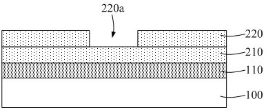
[0030] Step S100, a first material layer and a second material layer are formed on the substrate in sequence, a first window is opened in the second material layer, and the dielectric constants of the first material layer and the second material layer are the same. lower than the dielectric constant of silicon nitride.
[0031] Step S200, forming a mask spacer on the sidewall of the first window, and defining a second window by the mask spacer.
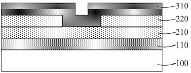
[0032] Step S300, removing the portion of the first material layer exposed to the second window to form a third window in the first material l...
PUM
 Abstract
Description
Claims
Application Information
 - R&D Engineer
- R&D Manager
- IP Professional
- Industry Leading Data Capabilities
- Powerful AI technology
- Patent DNA Extraction
Browse by: Latest US Patents, China's latest patents, Technical Efficacy Thesaurus, Application Domain, Technology Topic, Popular Technical Reports.
© 2024 PatSnap. All rights reserved.Legal|Privacy policy|Modern Slavery Act Transparency Statement|Sitemap|About US| Contact US: help@patsnap.com