Wave-absorbing surface with low profile and low incidence angle sensitivity and manufacturing process thereof

A technology of incident angle and sensitivity, applied in the direction of electrical components, antennas, etc., can solve the problems of incident angle sensitivity and high profile of absorbing materials

Pending Publication Date: 2021-09-14
YANGTZE DELTA REGION INST OF UNIV OF ELECTRONICS SCI & TECH OF CHINE HUZHOU
View PDF0 Cites 2 Cited by
  • Summary
  • Abstract
  • Description
  • Claims
  • Application Information

AI Technical Summary

Problems solved by technology

[0006] The purpose of the present invention is to overcome the shortcomings of the above-mentioned prior art, provide a low-profile and low-incidence-angle-sensitive wave-absorbing surface and its manufacturing process, and solve the problem of excessively high profile of the wave-absorbing material while ensuring the working performance of the wave-absorbing body. and the problem of being more sensitive to the angle of incidence

Method used


Image

  • Wave-absorbing surface with low profile and low incidence angle sensitivity and manufacturing process thereof
  • Wave-absorbing surface with low profile and low incidence angle sensitivity and manufacturing process thereof
  • Wave-absorbing surface with low profile and low incidence angle sensitivity and manufacturing process thereof

Examples


Embodiment Construction

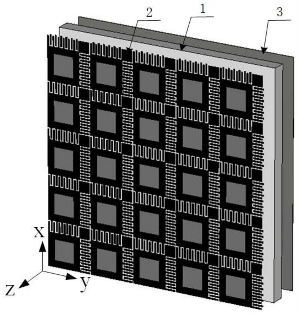
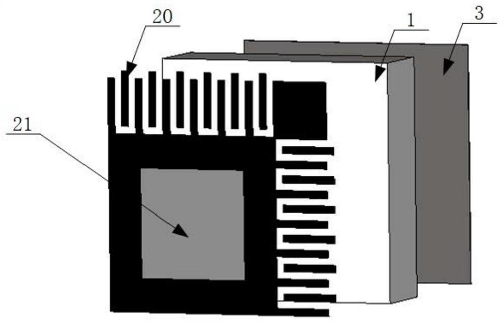
[0034] Such as Figure 1-4 As shown, the wave-absorbing surface with low profile and low incidence angle sensitivity of the present invention includes a dielectric substrate 1 , a two-dimensional planar periodic array 2 printed on the front of the dielectric substrate 1 , and a metal floor 3 printed on the back of the dielectric substrate 1 . The overall structure from top to bottom is a two-dimensional planar periodic array 2, a dielectric substrate 1, and a metal floor 3.

[0035] The two-dimensional planar periodic array (2) is formed by periodic arrangement of lossy frequency selection units along two directions of x-axis and y-axis.

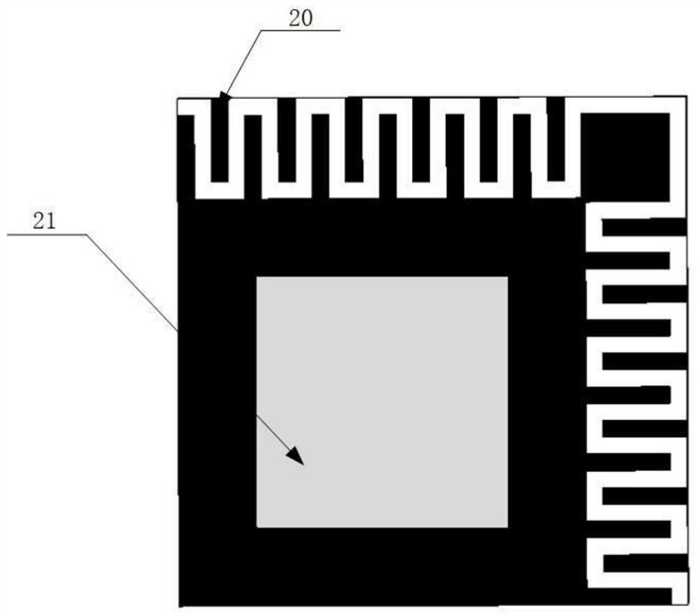
[0036] The lossy frequency selective unit of the two-dimensional planar periodic array 2 is a nested structure composed of an edge interdigitated resistive square ring patch and a metal square patch, and the metal square patch is embedded in the resistive square patch. The area on the lower left of the ring patch.

[0037] The edge of each...


PUM

PropertyMeasurementUnit
thicknessaaaaaaaaaa
thicknessaaaaaaaaaa

Abstract

The invention discloses a wave-absorbing surface with low profile and low incidence angle sensitivity. The wave-absorbing surface comprises a dielectric substrate, a two-dimensional plane periodic array printed on the front surface of the dielectric substrate and formed by arranging lossy frequency selection units, and a metal back plate, and the lossy frequency selection unit is formed by nesting a resistive square ring patch with an interdigital edge and a metal square patch. According to the invention, the wave absorbing rate can reach more than 90% in the working frequency band, and good performance stability can be maintained for incident electromagnetic waves with TE and TM polarization, a pitching incident angle in a range of 0-40 degrees and an incident angle in any direction. Compared with the prior art, the wave-absorbing surface has the advantages of being extremely low in profile, light in weight, convenient to process, high in wave absorbing rate in a working frequency band, good in polarization stability and angle stability and good in engineering application prospect.

Description

technical field [0001] The invention belongs to the technical field of microwave and millimeter wave antennas, and relates to a wave-absorbing surface with low profile and low incidence angle sensitivity and a manufacturing process thereof. Background technique [0002] Absorbing materials refer to electromagnetic materials and electromagnetic structures that can attenuate, lose, and absorb electromagnetic waves. Through the loss of materials, electromagnetic wave energy in the microwave frequency band is converted into heat energy or other forms of energy. It is widely used in radar stealth, electromagnetic compatibility / shielding, and antennas. field of design. According to the working principle of the absorber, the resonant frequency of the absorber can be reduced by increasing the capacitance between adjacent patches. If you want to correct the resonant frequency of the absorber to the original position, you need to reduce the thickness of the dielectric substrate. , th...

Claims


Application Information

Patent Timeline
Patent Type & Authority Applications(China)
IPC IPC(8): H01Q17/00
CPCH01Q17/008
Inventor 杨歆汨汤思宇张颖黄晨路万家辉陈志
Owner YANGTZE DELTA REGION INST OF UNIV OF ELECTRONICS SCI & TECH OF CHINE HUZHOU
Why Eureka
Try Eureka