

Switching power supply device
A technology of switching power supply and switching element, which is applied in the direction of output power conversion devices, electrical components, and adjusting electrical variables, which can solve the problems of insufficient phase margin and unstable operation.
- Summary
- Abstract
- Description
- Claims
- Application Information
AI Technical Summary
Problems solved by technology
Method used
Image

Examples
Embodiment 1
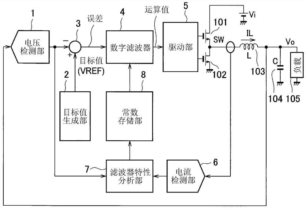
[0034] figure 1 It is a circuit configuration diagram of the switching power supply device of the first embodiment. figure 1 The switching power supply device of Embodiment 1 shown has a voltage detection unit 1, a target value generation unit 2, a subtractor 3, a digital filter 4, a drive unit 5, a current detection unit 6, a filter characteristic analysis unit 7, and a constant storage unit. 8. High-side MOSFET 101 , low-side MOSFET 102 , inductor 103 , output capacitor 104 and output load 105 . The high-side MOSFET 101 and the low-side MOSFET 102 correspond to switching elements of the present invention.
[0035] The switching power supply device converts the first DC voltage supplied from the power supply Vi into the second DC voltage via the inductor 103 and the output capacitor 104 by turning on and off the high-side MOSFET 101 and the low-side MOSFET 102 alternately, and supplies the output voltage to the output voltage. The load 105 supplies the output voltage Vo.
...
Embodiment 2
[0081] Figure 9 It is a configuration diagram of the switching power supply device of the second embodiment. Compared with the first embodiment, the second embodiment has a constant calculation unit 9 instead of the constant storage unit 8 . The other configurations of the second embodiment are the same as those of the first embodiment, so only the constant calculation unit 9 will be described.
[0082] The constant calculation unit 9 is based on the filter characteristic analysis result (LC resonance frequency f 0 value), the target crossover frequency fca, the target phase margin PMa and other information required for setting, calculate the filter constant satisfying the condition, and apply the calculated filter constant to the digital filter 4 . An example of the calculation method in the constant calculation unit 9 will be described.
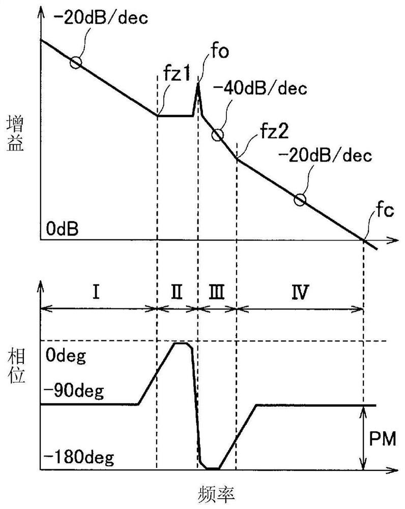
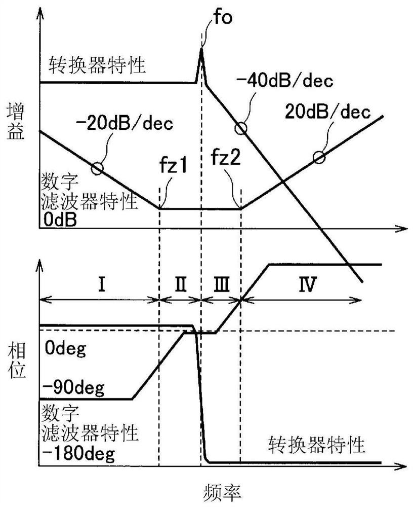
[0083] When it is assumed that the optimized filter characteristics satisfy fz 1 0 2 2 .
[0084] fz 2 ≒-fca·tan(PMa+90deg)-fz 1 ....
Embodiment 3
[0095] Figure 10 It is a configuration diagram of the switching power supply device of the third embodiment. In the switching power supply device of the third embodiment, an input voltage detection unit 10 is added to the switching power supply device of the second embodiment. In addition, the digital filter 4 is changed to a digital filter 4b. Figure 10 The other structures shown are the same as figure 1 The structures shown are the same, so only the different structures are described.
[0096] The input voltage detection unit 10 detects the input voltage Vi, and outputs the detected input voltage Vi as a digital value to the digital filter 4b. The digital filter 4 b outputs to the drive unit 5 an analysis signal that changes in accordance with the value of the input voltage Vi detected by the input voltage detection unit 10 during the filter characteristic analysis period Tr. The drive unit 5 controls the high-side MOSFET 101 and the low-side MOSFET 102 at a duty ratio...
PUM
 Abstract
Description
Claims
Application Information