Wafer fork, silicon wafer transfer device and method

A handover device and chip fork technology, which is used in electrical components, semiconductor/solid-state device manufacturing, circuits, etc., can solve problems such as deformation and damage of silicon wafers, achieve good adsorption effect, improve transmission efficiency, product accuracy, and accurate handover positioning. Effect

Pending Publication Date: 2021-09-28
SHANGHAI MICRO ELECTRONICS EQUIP (GRP) CO LTD
View PDF0 Cites 0 Cited by
  • Summary
  • Abstract
  • Description
  • Claims
  • Application Information

AI Technical Summary

Problems solved by technology

[0004] The purpose of the present invention is to provide a chip fork, silicon chip transfer device and method to solve the technical problem existing in the prior art that when the chip fork absorbs a silicon chip in a certain groove, it will cause deformation and damage to the silicon chip in the adjacent groove

Method used


Image

  • Wafer fork, silicon wafer transfer device and method
  • Wafer fork, silicon wafer transfer device and method
  • Wafer fork, silicon wafer transfer device and method

Examples


Embodiment 1

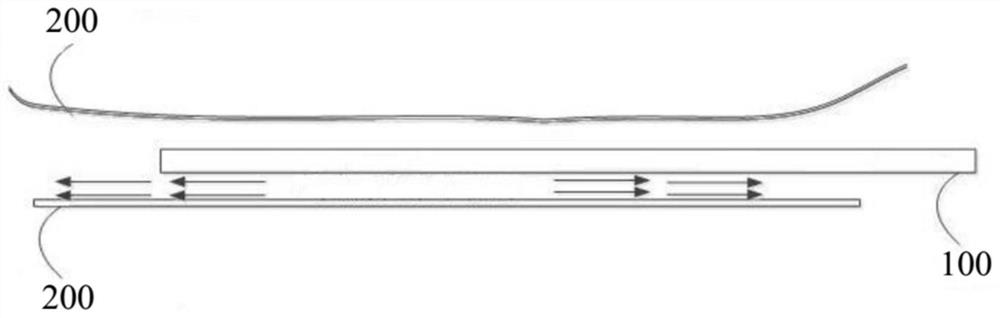
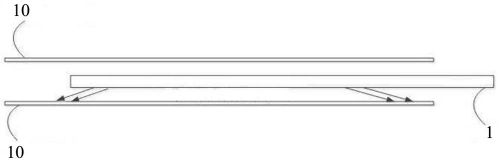
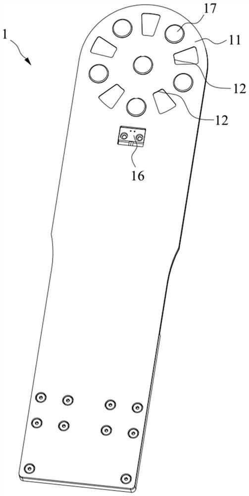
[0052] see figure 2 and image 3 , the embodiment of the present invention provides a fork for absorbing silicon wafer 10 . The chip fork 1 includes a chip fork body, and the chip fork body has an adsorption surface 11 for absorbing the silicon wafer 10. The adsorption surface 11 is provided with a plurality of air outlet holes 12, and the gas ejected from the plurality of air outlet holes 12 is inclined toward the outside of the adsorption surface 11. In order to reduce the air pressure on the adsorption surface 11, the Bernoulli effect is used to form a positive pressure adsorption area to adsorb the silicon wafer 10. Since the jetting direction of the gas is inclined, when the silicon wafer 10 in a certain groove is adsorbed, the silicon wafer 10 in an adjacent groove will not be deformed and damaged. Arrows in the drawings show the direction of gas flow.

[0053] Since the silicon wafer 10 is mostly circular, the adsorption surface 11 has a central position, and a plur...

Embodiment 2

[0078] Figure 10 to Figure 13 Embodiment 2 is shown, in which components identical or corresponding to those in Embodiment 1 are identified with reference numerals corresponding to Embodiment 1. For simplicity, only the differences between Embodiment 2 and Embodiment 1 are described. The difference is that the slope 14 is connected to the adsorption surface 11 and is located downstream of the gas outlet 12 , and the gas flows from the gas path 13 to the gas outlet 12 along the slope 14 . The structure of the air passage 13 and the air outlet 12 is simplified, which is convenient for processing and production.

[0079] In this embodiment, the extension direction of the air passage 13 is parallel to the adsorption surface 11, and the gas injection direction of the air outlet hole 12 is parallel to the adsorption surface 11. Due to the setting of the inclined surface 14, the gas ejected from the air outlet hole 12 is inclined relative to the adsorption surface 11. flow. exist...

Embodiment 3

[0084] For simplicity, only the differences between Embodiment 3 and Embodiment 1 are described. The difference is that along the direction of gas flow, the flow area of ​​the gas path 13 decreases gradually, so that the gas flow speed is accelerated, and a stronger Bernoulli effect is formed on the adsorption surface 11, which is more conducive to stably adsorbing the silicon wafer 10 .

[0085] In Embodiment 1, when the inclined surface 14 is located at the intersection of the air passage 13 and the air outlet 12 , due to the setting of the inclined surface 14 , the cross-sectional shape of the air passage 13 changes from a rectangle to a triangle, and the flow area gradually decreases. Using the slope not only makes the injection direction of the gas inclined, but when the silicon wafer in a certain groove is adsorbed, it will not cause deformation and damage to the silicon wafer in the adjacent groove; and the flow area of ​​the gas path 13 is gradually reduced, and the flow ...


PUM


Abstract

The invention discloses a wafer fork, a silicon wafer transfer device and method, and belongs to the technical field of semiconductors, wherein the wafer fork comprises a wafer fork body; the wafer fork body is provided with an adsorption surface for adsorbing a silicon wafer, the adsorption surface is provided with a plurality of gas outlet holes, and gas ejected from the plurality of gas outlet holes inclines towards the outer side of the adsorption surface. As the spraying direction of the gas is inclined, when a silicon wafer in a certain groove is adsorbed, the silicon wafer in an adjacent groove is not deformed and damaged. The silicon wafer transfer device comprises the wafer fork, a workbench and a shifting mechanism, a negative pressure adsorption area is formed on the workbench, and the shifting mechanism is used for driving the wafer fork to move. The silicon wafer transfer method comprises the steps that the gas outlet inclinedly sprays gas to form the positive pressure adsorption area, and the negative pressure adsorption area is matched with the positive pressure adsorption area, so that transfer positioning of the silicon wafer is accurate, the silicon wafer does not shift, and the conveying efficiency and the product precision are improved.

Description

technical field [0001] The invention relates to the technical field of semiconductors, in particular to a die fork and a silicon die transfer device and method. Background technique [0002] In the semiconductor industry, the transfer and positioning of silicon wafers is an important part of processing and production. In the prior art, the fork is generally driven by a manipulator to move, and an air hole is provided on one side of the fork, which can spray air outward to generate adsorption force, and can absorb the silicon wafer, thereby realizing the movement and transmission of the silicon wafer. [0003] The existing chip fork, the working principle is as follows figure 1 As shown, the air outlet direction of the air hole is parallel to the surface of the sheet fork 100. When the sheet fork 100 sucks the silicon wafer 200 in the nth groove, due to the horizontal flow of the air flow, the silicon wafer 200 in the n+1th groove above the silicon wafer 200 in the nth groov...

Claims


Application Information

Patent Timeline
Patent Type & Authority Applications(China)
IPC IPC(8): H01L21/683
CPCH01L21/6838
Inventor 刘凯王刚董洪波
Owner SHANGHAI MICRO ELECTRONICS EQUIP (GRP) CO LTD
Why Eureka
Try Eureka